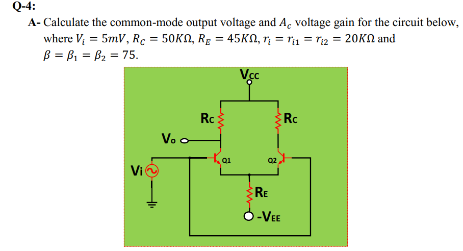
- Calculate the common-mode output voltage and A. voltage gain for the circuit below, where V; = 5mV, Rc = 50K, RĘ = 45KN, rị = ri1 = riz = 20KN and ß = B1 = B2 = 75. Vcc Rc Rc Vo o Q2 Vi RE O-VEE


Q: 1.3 Output Resistance: For Vcc higher than Vomin, calculate the output resistance Ro of the current…
A: Given the circuit: For Vcc higher than Vo,min we need to calculate the output resistance Ro.…
Q: 5. Calculate the common-mode output voltage for the circuit given that Vi=5mV, Rc=50kohm and…
A: we need to determine common mode output voltage for the given circuit.
Q: |a- Design a circuit with the following output using two opamps at least. Use three resistor (a=7,…
A: (a) Write the given output voltage expression and substitute the known values.…
Q: the signal cult thal amp). i. List out the type of signal conditionings involved in the circuit.…
A: Solution- Signal conditioning - It is the manipulation of the signal, it amplifies the signal from…
Q: 21:Choose the values of Rp. Rs and RL for the JFET amplifier circuit in figure that will result in…
A: Given,Av=18.062dBIDSS=8mA, Vp=-5V, VDQVDD=0.375IDQIDSS=0.25Now, IDQIDSS=1-VGSVP=0.447⇒…
Q: Figure below shows a circuit for an instrumentation operational amplifier which has a voltage gain…
A: 1) When SW1 switch is open then the current through R1 is zero and equivalent circuit diagram will…
Q: b) When setting the Q-point of a JFET amplifier why is the bias circuit show in Figure 3.1 (b) used…
A: b. To stabilize the Q-point (operating point) bias the circuit. We know that JFET input resistance…
Q: 2.2 Which of the following Common Source Amplifier's general one of its features. A) The voltage…
A:
Q: a. For the circuit shown in Figure1, given that Rc = 3 KO, R L=1KN, V cc = 15 V, voltage gain Av=10v…
A:
Q: Determine V, and the common-mode voltage gain Ac in the circuit shown in Figure 1. 10V R5 R4 10k2…
A: Assume β>>1 so base current equal to zero IB=0. Use the voltage divider rule, to find the base…
Q: Q-4: A- Calculate the common-mode output voltage and A, voltage gain for the circuit below, where V…
A:
Q: The parameters of the circuit shown in the Figure are: V* = 4.4V, V¯ = -4.4V, and VBB = 0V. The…
A: Given :VBB=0VV+=4.4VV-=-4.4VVBE=0.7Vβ=80
Q: The ---- amplifier configuration has the highest input resistance compared to the other…
A: In this question , we will find which configuration has high input resistance ...
Q: Q1: Choose the correct answer. Each question weighted Si transistor has ICEO = 0, B = 100, Rc= 2k2,…
A: The correct option is 1st 1.55 I have also solved all the other parts as well for the reference
Q: Determine V, and the common-mode voltage gain Ac in the circuit shown in Figure 1. 10V R5 10KQ R4…
A: The circuit is, Assume β>>1 so base current equal to zero IB=0. Use the voltage divider…
Q: Q 4. For the given biasing configuration in figure D, determine the following parameters: а. Ic b.…
A: Given data: VCC=18 VVC=12 VRC=4.7 kΩRE=1.2 kΩ Solution: (a) VCC-VC=IC×RC 18-12=IC×4700…
Q: For the Amplifier circuit of figure. The transistor has a ß of 800. The mid band voltage gain V, /V,…
A: The given circuit is in a common collector configuration. The ideal voltage gain of the common…
Q: Q4. For the inverting amplifier shown in Figure 5 find the voltage gain Vo of the circuit. 10 K 100…
A:
Q: QUESTION 4: The following figure shows a basic two-transistor pnp current source. The transistor…
A:
Q: For a self biased circuit shown in figure, calculate voltage gain, input and output resistances and…
A:
Q: shows a well-known circuit configuration with the bypassed source resistor using an n-channel…
A: You have posted so many sub part of questions , as per our company guidelines we are supposed to…
Q: A lead network shown in the figure is designed to compensate the drop in the gain for a biopotential…
A:
Q: s1) a) What area does the circuit run in? Calculate the middle band voltage gain Av=? VA=303V,…
A:
Q: In the bridge type circuit shown in Figure below, Find: F 10:1 а. d.c. оutput Current D3. D1 and…
A: Given Data: Vrms = 115 V Fin = 50 Hz RL = 2200 ohm
Q: 1312 Q.25: For the linear transfomer circuit 1:5 shown: 12,00y 1. Find the value of V,, V2, 4 & ? 2.…
A:
Q: Q2 Vin - R2 R3 RL Vout
A: Given circuit is series regulator Power = VCE *ICE we can find power
Q: Calculate the closed loop gain for the following circuit. Assume A0 for both transistors and Ry+ R2…
A: Given small signal circuit with open dc current source open dc voltage source.
Q: Consider the circuit shown in Figure 2. The transistor parameters are ß= 100 and VA 100 V. Determine…
A: For the above given question we need to calculate the value of input impedance, voltage and current…
Q: ay be preferable in certain situations. Analytically determine the "gain" of the non-inverting…
A:
Q: For the circuit shown below, if the voltage across Re is to be 250mV with a transconductance gm =…
A: For the circuit shown below If the voltage across RE is to be 25o mV with a transconducatnce gm=1/26…
Q: Vec +12V Re 1kS2 Re 470k2 BC107 Vc Ve Figure 3: Practical Fixed Bias Transistor Circuit 2. Measure…
A: Dear student as per our guidelines we are supposed to solve only one question.kindly repost other…
Q: Calculate the output voltage of a noninverting amplifier for values of V = 12v, Rf = 500kN, and R1…
A: Draw the configuration of non inverting amplifier and than write the input output relation. For…
Q: Calculate the closed-loop gain Vo/Vs when Vs = 1V. Vo/Vs = io 741 + Vs Μ 5 ΚΩ ww 40 ΚΩ 20 ΚΩ Μ
A: The solution is given below
Q: For the rotage feedback nehoork of Figure a) Ic BOV 3) Vc c) VE -l) Vce 8.2KN 330ke 220k Ve Ie +…
A: It is given that:
Q: e are six parts. Use the first circuit diagram for the first three parts and the second circuit…
A:
Q: Rf Vin_1 W Rf Vin_1 W Ri Ri_1 TL074 Vout + TL074 Vout Vin_2 Ro Vin_2 W + R1 Ri_2 Ro R2 Figure C:…
A:
Q: Problem5: For the common base circuit shown in figure find I. and VCB. Assume transistor is Silicon…
A:
Q: 2. We want to design a boost converter that meets the following specifications: • Vo = 12V Vin 3.6…
A:
Q: Non Inverting Amplifier 1. Calculate the gain of a non-inverting amplifier shown in Figure 2. Av =…
A:
Q: The Pinch off voltage for N-Channel JFET is -3V, maximum saturated drain current 8mA and the value…
A:
Q: Instrumentation Amplifier Circuit 2R, 1+ R. V. V1 out RG R, (4-2) R2 R3 R1 RG Vout R2 R1 R3 V2 13
A: Note: We are authorized to answer one question at a time since you have not mentioned which question…
Q: 2 Q1// Calculate the output voltage (Vout) for the amplifier RF ww 1MQ R1 www 10kQ V1 1mV- R2 20kQ…
A: In this question we will find output voltage of given operational amplifier.....
Q: Consider the circuit shown. The transistor parameters are: B 100, VBE=0.7V, and VCE (SAT) = 0.2V.…
A: The solution is given below
Q: 0.7 V R3 4s BINARY INPUT 2s 4 1 R₂ 18.7 k Resistor network R₁ 37.5 k 1s 75 kn Input resistors…
A: The above diagram is that of a weighted resistor DAC. It uses weighted resistors in the inverting…
Q: Q.1: A- For circuit of Figure below, determine ICQ and VCEQ. B- Sketch the de load line. 18V 36K…
A:
Q: 3) With reference to the switching conditions given below develop an appropriate circuitry that can…
A: Introduction: Diode converters AC (Alternating current) supply in DC (Direct current) supply. This…
Q: na common emiter amplifier (Voltage Divider) with the following network R1 = 22k, R2 = 6.8k, Rc =…
A:
Q: Calculate the output voltage of an OPAMP summing amplifier for the following sets of voltage and…
A: Amplifiers are used to provide the amplified signal of the input signal. In a mic speaker setup, the…
Q: The transistors in figure below have the following parameter values: Qi: gml = 4 mS, rai 0, and Q2:…
A: Given data,
Q: V* = 10V Rg = 5kN R. - 20k R. R. = 3.19kN Pa o R. = 19.72 RL = 1 k2 R. 93.7N R, = 13.9N V- =-8V The…
A: Brief description : Here they have mentioned a common collector amplifier circuit. The…

Step by step
Solved in 3 steps with 3 images


- DESIGN AND SIMULATION OF A TWO-STAGETRANSISTOR AMPLIFIER USING LTSPICE TWO-STAGE INVERTING AMPLIFIER VOLTAGE GAIN ≥ 300 A. SCHEMATIC WITH COMPONENT VALUESB. SCHEMATIC OR CIRCUIT DISCUSSIONCalculate the output voltage of an op-amp summing amplifier for the followingsets, consider Rf=1Mna. V1=+1v, V2=+2v, V3=+3v, Ri=R2, R3=500Ω b. V1=+1v, V2=+2v, V3=+3v, Ri-500kΩ, R2=1MΩ, R3=1MΩFigure Q. 3(b) shows an op amp circuit for linear amplifier application. (i) Determine the value of current I3.(ii) Find the value of R if the output current, Io is given as 2 mA.(iii) Explain what will happen to output voltages, V01 and V02 if the supplyvoltages, +VCC and -VCC are connected to +10V and -10V.
- 3G Problem 1. (P1) Three op-amps are connected in cascade configuration. An 80 microVolts signal is connected to the non-inverting input of the first op-amp. Both the 2nd and 3rd op-amps operates as inverting amplifiers. All feedback resistors are 420 KOhms while the input resistances are 71.4kOhms, 19.1kOhms, and 14KOhms respectively. Determine the output voltage of the second stage stage. a.-2640 mV b.-26.4 mV c.-1.2 mV d.26 VAs a maintenance engineer in a semiconductor company, you are given a task to replace the current version of dc-biasing circuit for a faulty tester machine. This dc-biasing circuit used an n-channel JFET as shown in Figure 2. Re-design a new dc-biasing circuit using an n-channel D-MOSFET that can produce a similar output current, IDQ as the previous circuit. Your tasks are: (i) Calculate the operating point (IDQ and VGSQ) of the dc-biasing circuit in Figure 2. Then sketch the JFET network transfer curve (ID and VGS). (ii) Without changing the circuit configuration, calculate the values of source resistor, RS and RB to achieve this objective. Determine the commercial value of the new RS and RB. For cost reduction reason, the values of RD, RA and VDD should be maintained. The chosen D-MOSFET has a maximum drain current of 8 mA and gate-source cutoff voltage of – 15V. The new RS value should be 3 times larger than the old RS used in the JFET network to compensate for the high…3ZD Calculate the output voltage of an op-amp if a 100mV signal is applied to the non-inverting input of the op-amp circuit which has an Rf = 0 Ohms and Ri = 0 Ohms. a.Infinity Volts b.0 Volts c.1 Volts d.-2 Volts
- For the circuit in Figure A2, Vs = 6.7 V, Rout = 300 kΩ and RL = 100 kΩ. The operational amplifier is connected to DC voltages of +/- 12 V as the positive and negative voltage supply. Calculate the voltage across the load resistance RL.Calculate the voltage of an inverting op-amp summing amplifier for the following sets of resistors. Use Rf = 1 MΩ in all casesa) V1 = 1V, V2 = 2V, V3 = 3V, R1 = 500 kΩ, R2 = 1MΩ, R3 = 1 MΩb) V1 = -2V, V2 = 3V, V3 = 1V, R1 = 200 kΩ, R2 = 500 kΩ, R3 = 1 MΩ1. Give an example of how the traditional current-mode DAC will have limited output swing. 2. Show the detailed derivation of Eqs. (30.12)-(30.14).
- Determine the overall Voltage Gain Av and Current Gain of the circuit below given = 100, gm = 20 us, IDss = 10 mA and Vp = - 4V.Calculate the output voltage of an op-amp summing amplifier for the given values of voltages and resistors. Use Rf = 1 MΩ. V1 = 5.84V V2 = 8.47V V3 = 8.25V R1 = 482kΩ R2 = 0.58MΩ R3 = 1.31MΩ QUICKLYDetermine the output voltage of an op amp amplifier circuit with the following parameters: Differential voltage gain = 4522CMRR = 631Vi1 = 659 mV Vi2 = 659 mV Vi1 and Vi2 are in phase and have the same frequency. \ QUICKLY