Choose the correct answer: a) The reason of high input resistance of the MOSFET is: 1. The insulator layer. 2. The reverse biasing. 3. The forward biasing. b) Which transistor has no Ipss parameter?. 1. JFET. 2. E-MOSFET. 3. D-MOSFET. ¢) For an n-channel D-MOSFET transistor, at what condition can gm be greater than gmo?. 1. Vs is positive. 2. Vgs is negative. 3. Vas =0. d) A certain amplifier has an Rp=1KQ. When a load resistance of 1KQ is capacitively coupled to the drain, the gain will reduce to the: 1. Half. 2. Quarter. 3. Not change.
Choose the correct answer: a) The reason of high input resistance of the MOSFET is: 1. The insulator layer. 2. The reverse biasing. 3. The forward biasing. b) Which transistor has no Ipss parameter?. 1. JFET. 2. E-MOSFET. 3. D-MOSFET. ¢) For an n-channel D-MOSFET transistor, at what condition can gm be greater than gmo?. 1. Vs is positive. 2. Vgs is negative. 3. Vas =0. d) A certain amplifier has an Rp=1KQ. When a load resistance of 1KQ is capacitively coupled to the drain, the gain will reduce to the: 1. Half. 2. Quarter. 3. Not change.

Introductory Circuit Analysis (13th Edition)
13th Edition
ISBN:9780133923605
Author:Robert L. Boylestad
Publisher:Robert L. Boylestad
Chapter1: Introduction
Section: Chapter Questions
Problem 1P: Visit your local library (at school or home) and describe the extent to which it provides literature...

Related questions
Question
5. Choose the correct answer: a) The reason of high input resistance of the MOSFET is: 1. The insulator layer. 2. The reverse biasing. 3. The forward biasing. b) Which transistor has no Ipss parameter?. 1. JFET. 2. E-MOSFET. 3. D-MOSFET. ¢) For an n-channel D-MOSFET transistor, at what condition can gm be greater than gmo?. 1. Vs is positive. 2. Vgs is negative. 3. Vas =0. d) A certain amplifier has an Rp=1KQ. When a load resistance of 1KQ is capacitively coupled to the drain, the gain will reduce to the: 1. Half. 2. Quarter. 3. Not change.
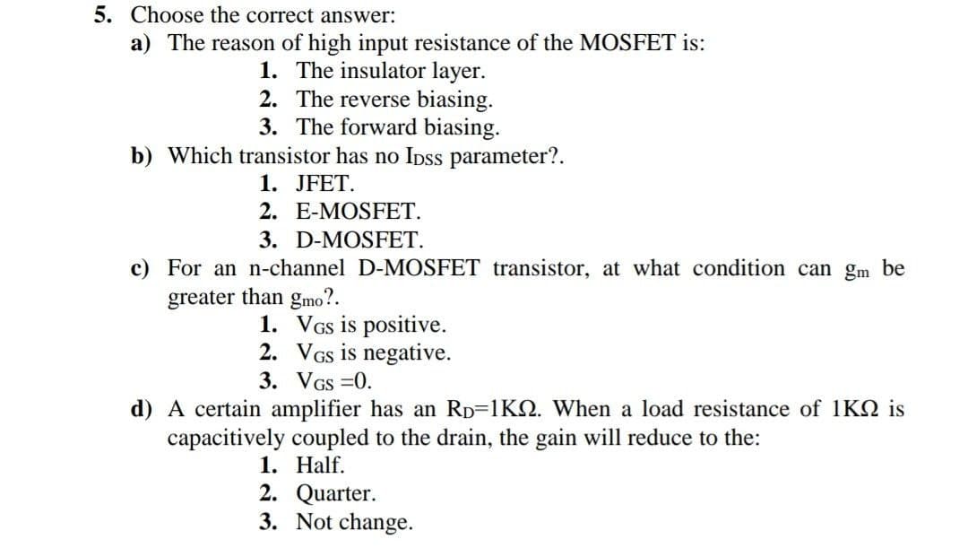
Transcribed Image Text:5. Choose the correct answer:
a) The reason of high input resistance of the MOSFET is:
1. The insulator layer.
2. The reverse biasing.
3. The forward biasing.
b) Which transistor has no Ipss parameter?.
1. JFET.
2. E-MOSFET.
3. D-MOSFET.
c) For an n-channel D-MOSFET transistor, at what condition can gm be
greater than gmo?.
1. VGs is positive.
2. VGs is negative.
3. VGS =0.
d) A certain amplifier has an RD=1K2. When a load resistance of 1KQ is
capacitively coupled to the drain, the gain will reduce to the:
1. Half.
2. Quarter.
3. Not change.
Expert Solution
This question has been solved!
Explore an expertly crafted, step-by-step solution for a thorough understanding of key concepts.

Step by step
Solved in 4 steps

Knowledge Booster


Learn more about
Need a deep-dive on the concept behind this application? Look no further. Learn more about this topic, electrical-engineering and related others by exploring similar questions and additional content below.Recommended textbooks for you
Introductory Circuit Analysis (13th Edition)
Electrical Engineering
ISBN:
9780133923605
Author:
Robert L. Boylestad
Publisher:
PEARSON

Delmar's Standard Textbook Of Electricity
Electrical Engineering
ISBN:
9781337900348
Author:
Stephen L. Herman
Publisher:
Cengage Learning

Programmable Logic Controllers
Electrical Engineering
ISBN:
9780073373843
Author:
Frank D. Petruzella
Publisher:
McGraw-Hill Education
Introductory Circuit Analysis (13th Edition)
Electrical Engineering
ISBN:
9780133923605
Author:
Robert L. Boylestad
Publisher:
PEARSON
Delmar's Standard Textbook Of Electricity
Electrical Engineering
ISBN:
9781337900348
Author:
Stephen L. Herman
Publisher:
Cengage Learning
Programmable Logic Controllers
Electrical Engineering
ISBN:
9780073373843
Author:
Frank D. Petruzella
Publisher:
McGraw-Hill Education

Fundamentals of Electric Circuits
Electrical Engineering
ISBN:
9780078028229
Author:
Charles K Alexander, Matthew Sadiku
Publisher:
McGraw-Hill Education

Electric Circuits. (11th Edition)
Electrical Engineering
ISBN:
9780134746968
Author:
James W. Nilsson, Susan Riedel
Publisher:
PEARSON

Engineering Electromagnetics
Electrical Engineering
ISBN:
9780078028151
Author:
Hayt, William H. (william Hart), Jr, BUCK, John A.
Publisher:
Mcgraw-hill Education,