Considering the operational amplifier circuit below, the values of R1=20KO, R2=1KO, R3=20KO and Ra=1KO. If V1=7 V and Vz=5, then the output voltage Vu equals R3 R2 V1 W Vout V20 R1
Considering the operational amplifier circuit below, the values of R1=20KO, R2=1KO, R3=20KO and Ra=1KO. If V1=7 V and Vz=5, then the output voltage Vu equals R3 R2 V1 W Vout V20 R1

Delmar's Standard Textbook Of Electricity
7th Edition
ISBN:9781337900348
Author:Stephen L. Herman
Publisher:Stephen L. Herman
Chapter18: Resistive-inductive Parallel Circuits
Section: Chapter Questions
Problem 13PP: In an R-L parallel circuit, IT=1.25 amps, R=1.2k, and XL=1k. Find IR

Related questions

Question
100%
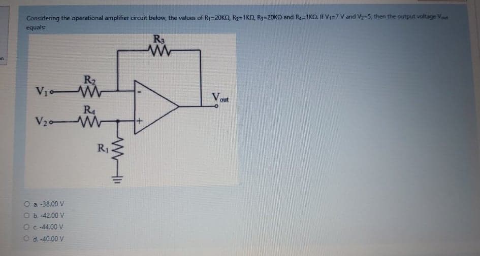
Transcribed Image Text:Considering the operational amplifier circuit below, the values of R1=20KN, R2=1KO, R3=20KO and Ra=1KO. If V1=7 V and V2=5, then the output voltage Vut
equals
R3
on
R2
V1 W
V out
R4
V20 W
R1
O a. -38.00 V
O b. -42.00 V
O c -44.00 V
O d. -40.00 V
Expert Solution
This question has been solved!
Explore an expertly crafted, step-by-step solution for a thorough understanding of key concepts.

Step by step
Solved in 2 steps with 1 images

Knowledge Booster


Learn more about
Need a deep-dive on the concept behind this application? Look no further. Learn more about this topic, electrical-engineering and related others by exploring similar questions and additional content below.Recommended textbooks for you
Delmar's Standard Textbook Of Electricity
Electrical Engineering
ISBN:
9781337900348
Author:
Stephen L. Herman
Publisher:
Cengage Learning
Delmar's Standard Textbook Of Electricity
Electrical Engineering
ISBN:
9781337900348
Author:
Stephen L. Herman
Publisher:
Cengage Learning