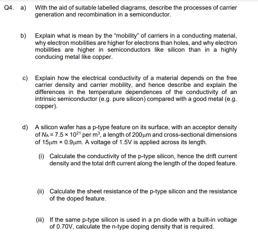
d) A silicon wafer has a p-type feature on its surface, with an acceptor density of NA = 7.5 × 10²¹ per m³, a length of 200μm and cross-sectional dimensions of 15μm x 0.9μm. A voltage of 1.5V is applied across its length. (i) Calculate the conductivity of the p-type silicon, hence the drift current density and the total drift current along the length of the doped feature. (ii) Calculate the sheet resistance of the p-type silicon and the resistance of the doped feature. (iii) If the same p-type silicon is used in a pn diode with a built-in voltage of 0.70V, calculate the n-type doping density that is required.
d) A silicon wafer has a p-type feature on its surface, with an acceptor density of NA = 7.5 × 10²¹ per m³, a length of 200μm and cross-sectional dimensions of 15μm x 0.9μm. A voltage of 1.5V is applied across its length. (i) Calculate the conductivity of the p-type silicon, hence the drift current density and the total drift current along the length of the doped feature. (ii) Calculate the sheet resistance of the p-type silicon and the resistance of the doped feature. (iii) If the same p-type silicon is used in a pn diode with a built-in voltage of 0.70V, calculate the n-type doping density that is required.
Power System Analysis and Design (MindTap Course List)
6th Edition
ISBN:9781305632134
Author:J. Duncan Glover, Thomas Overbye, Mulukutla S. Sarma
Publisher:J. Duncan Glover, Thomas Overbye, Mulukutla S. Sarma
Chapter4: Transmission Line Parameters
Section: Chapter Questions
Problem 4.2P: The temperature dependence of resistance is also quantified by the relation R2=R1[ 1+(T2T1) ] where...
Related questions
Question
Q4 part d please

Transcribed Image Text:Q4. a) With the aid of suitable labelled diagrams, describe the processes of carrier
generation and recombination in a semiconductor.
b)
Explain what is mean by the "mobility" of carriers in a conducting material,
why electron mobilities are higher for electrons than holes, and why electron
mobilities are higher in semiconductors like silicon than in a highly
conducing metal like copper.
c) Explain how the electrical conductivity of a material depends on the free
carrier density and carrier mobility, and hence describe and explain the
differences in the temperature dependences of the conductivity of an
intrinsic semiconductor (e.g. pure silicon) compared with a good metal (e.g.
copper).
d) A silicon wafer has a p-type feature on its surface, with an acceptor density
of NA = 7.5 × 10²1 per m³, a length of 200μm and cross-sectional dimensions
of 15μm x 0.9μm. A voltage of 1.5V is applied across its length.
(i)
Calculate the conductivity of the p-type silicon, hence the drift current
density and the total drift current along the length of the doped feature.
(ii) Calculate the sheet resistance of the p-type silicon and the resistance
of the doped feature.
(iii) If the same p-type silicon is used in a pn diode with a built-in voltage
of 0.70V, calculate the n-type doping density that is required.
Expert Solution
This question has been solved!
Explore an expertly crafted, step-by-step solution for a thorough understanding of key concepts.
Step by step
Solved in 4 steps with 4 images

Knowledge Booster
Learn more about
Need a deep-dive on the concept behind this application? Look no further. Learn more about this topic, electrical-engineering and related others by exploring similar questions and additional content below.Recommended textbooks for you

Power System Analysis and Design (MindTap Course …
Electrical Engineering
ISBN:
9781305632134
Author:
J. Duncan Glover, Thomas Overbye, Mulukutla S. Sarma
Publisher:
Cengage Learning

Power System Analysis and Design (MindTap Course …
Electrical Engineering
ISBN:
9781305632134
Author:
J. Duncan Glover, Thomas Overbye, Mulukutla S. Sarma
Publisher:
Cengage Learning