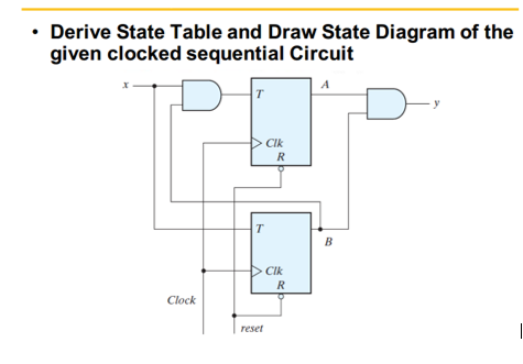
• Derive State Table and Draw State Diagram of the given clocked sequential Circuit CIk R т B Clk


Q: Consider the logic diagram and the timing diagram of the inputs X and Y graph below and answer the…
A: Timing diagrams are UML interaction diagrams used to show interactions when a primary purpose of the…
Q: 1. The following combinational circuit logic diagrams are given; find the output function and truth…
A: In mathematics and logic, a Boolean function is a function whose arguments, as well as the function…
Q: 3. Design a Full Adder circuit having the inputs as A, B and Cin. The output shoul Carry_Out.…
A: Designed a full adder circuit with A,B and Cin
Q: 2) Write VHDL code of the circuit as shown in figure INV AND2 AND2 X2 XOR2 OR3
A: Answer:-
Q: a) Draw the graphic symbol (block diagram) of SR Flip Flop on page. Mention/label all inputs and…
A: GIVEN: a) Draw the graphical symbol of SR flip flop. b) Draw the characteristic table c) Draw the…
Q: Derive the simplest state diagram and state table of a Moore-type FSM that has one nput w and one…
A:
Q: Given the expression below, build the equivalent digital circuit NAND implementation. X = AB + CB +…
A: We have first simplified the expression to perform NAND operation in between operands then , that…
Q: 1. Analyze the following sequential circuit Derive the (a) state equations (b) state table and (c)…
A: GIVEN:
Q: Q: Design a combinational circuit with four inputs lines that represent a decimal digit in BCD and…
A: Since you have asked multiple questions, according to the company's policy we will solve the first…
Q: Question 7 A lto 4 De-multiplexer is represented by the following block diagram, build the…
A: Here in this question we have given a 1*4 demux and we have asked to find truth table for this and…
Q: Analyze the given combinational circuit and answer the following questions. 1.) After obtaining the…
A:
Q: A' A B' B Clk Clk T T Clock
A: The given circuit is Mod 3 counter using T flip flop. Which repeatedly count 0,1,2,0,1,2,... State…
Q: Problem: Draw the RC equivalent circuit for the logic function below and calculate the falling and…
A: Logical RC equivalent circuit.......
Q: Transfer the given logic gate circuit with the inputs A, B, and C and the outputs Y and Z, according…
A: Below is the answer to above question. I hope this will be helpful for you...
Q: Q2. a) Derive the excitation equations and gutput equation for the following circuit (Figure 1).…
A:
Q: öislg äbäi A synchronous state machine has two inputs (X1 and X2) and one output (Z). The…
A: The solution to the given problem is below.
Q: a) Draw the state table of the synchronous sequential circuit, b) Derive the next state equations…
A: Answer in Step 2.
Q: Problem 3 Complete a truth table for the following transistor-level circuit. A B OUT 1 1 1 1
A: A transistor can be used to enable an IC connected to a low voltage supply to switch the current for…
Q: (a) Given the Boolean expression F(w,x.y,z)=wy'z+ x'y'z+w°xy+wx'y+ wxy. Design the circuit using 8×1…
A: Truth Table: W X Y Z Output 0 0 0 0 F 0 0 0 1 T 0 0 1 0 F 0 0 1 1 F 0 1 0 0 F 0 1 0…
Q: Draw an ASM chart and state diagram for the circuit shown in Figure 15.36. D. Z utput X input Q, Do…
A: Question :-
Q: B) Using positive edge T Flip Flop design synchronous circuit for the following state diagram? " 111…
A: BElow is the answer to above question. I hope this will be helpful for you...
Q: Design a 4:1 MUX in multiple ways: a) Using basic gates b) Using tri-state logic c) Using 2:1 MUXes…
A: 4:1 MUX: 4x1 Multiplexer has four data inputs( assume) I3, I2, I1 & I0, two selection lines…
Q: 1. Obtain a state diagram for a Moore circuit which produces output 1 when it detects the sequence…
A:
Q: Please explain all stepsSee attachment
A: For, first logic gate OR required Boolean expression is:(X OR Y) For, second logic gate XOR…
Q: FIGURE 11.55 is a state transition diagram for a sequential circuit with three flip-flops and one…
A: To design a sequential circuit with three flip-flops and one input that counts up in binary when the…
Q: Q2. A Mealy sequential circuit has one input, one output, and two flip-flops. A timing diagram for…
A: Given The answer is given below
Q: You are requested to analyze and design the sequential circuit according to the following given…
A: Given :
Q: Q. Draw the 3 x 3 Programmable Array Logic (PLA) with the statement for the following state diagram…
A: Let us draw the truth table first 3a. Implementation in PLA 3b. Implementation in PROM
Q: Design a combinational circuit with four inputs and represents a decimal digit in BCD and four…
A: Question :- Design a combinational circuit with four inputs and represents a decimal digit in BCD…
Q: A R T CLK Reset
A: Given The answer is given below Input equations:
Q: Given the sequential circuit, derive the state table and state diagram. K Q'F FFO X JQ K Q'F FF1 D…
A: Answer is given below-
Q: 4) Design a combinational logic circuit using 4 to 1 MUX with four-bit number as input, A, B, C,D…
A: The truth table is A B C D P Q R S 0 0 0 0 1 1 1 1 0 0 0 1 1 1 1 0 0 0 1 0 1 1 0 1 0 0…
Q: mp-nop'states. 11. Draw the logic diagram and the state transition diagram for a sequential circuit…
A:
Q: From the given circuit, derive the simplified NOT-OR-AND circuit and identify the TTL ICs in the…
A: The simplified NOT-OR-AND circuit The TTL ICs are NAND and NOR gate. Here 4 TTL ICs was being used…
Q: (b) Design a combinational circuit that will convert BCD to Excess 4 code with necessary steps.
A: Combinational logic is a type of digital logic which is implemented by boolean circuits where the…
Q: A Moore sequential circuit has one input and one output. The output should be 1 if the total number…
A: Moore sequential circuit is a type of Finite Automata which contain output to the given input. In…
Q: Derive the state table and the state diagram of the sequential circuit shown in Fig. P5.8 . Explain…
A: Draw the circuit for a flip-flop. If the input is high, then the flip-flop changes its state…
Q: Consider the following sequential circuit. Determine its state table and state diagram. Cp K 10
A: Given sequential circuit contains 2 J-K flip flops and there is one input. First flip flop's output…
Q: erive State Table and Draw State Diagram of the iven clocked sequential Circuit Clk K B Clk Dt K
A:
Q: 1. Explain using diagram how NOR and NAND Gates are Universal Gate. 2. What do you mean by…
A: 1. NAND and NOR gates are called as universal gates. Because with help of these gates any logica…
Q: 1. Design a combinational circuit with four input lines (W,X,Y,Z) that represent a decimal digit in…
A:
Q: Given the Boolean function: F1(X, Y, W, Z) = (0,1,2,4,5,6,8,9,12,13,) 1. Construct the truth table.…
A: 1. Truth table X Y W Z Output 0 0 0 0 1 0 0 0 1 1 0 0 1 0 1 0 0 1 1 0 0 1 0 0 1 0 1…
Q: Design a NAND Logic Circuit that is equivalent to the AOI circuit shown below: A B Z = BC +AC
A:
Q: a) Derive the state diagram, describe the meaning of each state clearly. Specify the type of the…
A: Please check the step 2 for solution
Q: Given f (w, x, y, z) = II(0, 1,3, 5, 13), %3D the cl b) E c) W d) Write Y = f(w, x, y, z) in SOP…
A: In Sum Of Products form, the low value(0) is written with a bar while the high value(1) is written…
Q: 1. For the circuit in Figure 1, determine the characteristic table. What is the cost of the circuit?…
A: Flipflop means, the user able to change it's value and the user able to save it forever. In SR…
Q: ii) For the circuit shown in figure (Q5-ii), deduce the state diagram for the circuit. 10₂ De D₁ D₂…
A: Given circuit is a sequential circuit which contains three D flip flops. For each flipflop, clock…
Q: Create a circuit for detecting 1110 in a sequential machine. In the process draw the state diagram…
A: Sequential Diagram
Q: Design a 4:1 MUX in multiple ways: a) Using basic gates b) Using tri-state logic c) Using 2:1 MUXes…
A:
Q: 2. The 74147 IC has an active low BCD outputs. What does active low means in digital circuits? 3.…
A: In digital circuits the term 'active low' means that the signal will be performing its function when…

Step by step
Solved in 2 steps with 2 images


- draw a QPSK demodulator circuit using different circuit components. stop rejecting questionsDesign the simplest circuit that has three inputs, a, b, and c, which returns an output value of 1 whenever g and b are complements of each other or b and c are complements of each other, otherwise the output is 0. Realize the circuit using 4input , 3output PALDraw the circuit diagram to output F given in the expression above by referring to schematics for 2-2) and 2-3). Use the space below to draw both the IC with pin assignments and a circuit schematic. Using a single 7400 IC construct a circuit to output the following Boolean function: F = AB + CD
- Identify the state diagram operation and find its output sequence for the following input sequence X=0101-1100-101-0000 the circuit accepts input bits from LSB to MSBdraw a qpsk complete modulator circuit using circuit components of various types not a block diagram.Draw the logic diagram of the digital circuit specified by the following Verilog description: module Circuit_C (y1, y2, y3, a, b);output y1, y2, y3;input a, b;assign y1 = a || b;and (y2, a, b);assign y3 = a && b;endmodule
- Q1 Using a multiplexer design a combinational circuit design defined by the following boolean expression: F= y'z'+x'y+yzDraw a Moore machine for a 1965 Ford Thunderbird, a car that featured sequentially flashing tail lights. Define the inputs/outputs of the circuit and draw a state diagram. (There should be 12 states). As soon as possible!Draw a state diagram for an FSM without inputs. Three outputs include a, b, and c. abc must exhibit the following sequence: 000, 001, 010, 100, repeat. The output only changes on a rising clock edge. The initial state must be 000.
- Distinguish between combinational logic circuits and sequential logiccircuits. How the design requirements of combinational circuits DOES specify?What are the differences between a combinational circuit and a sequential circuit?F =A'BC'+A'CD'+ACD+AB'C'D' Draw the Logic Gates diagram please Need Asap