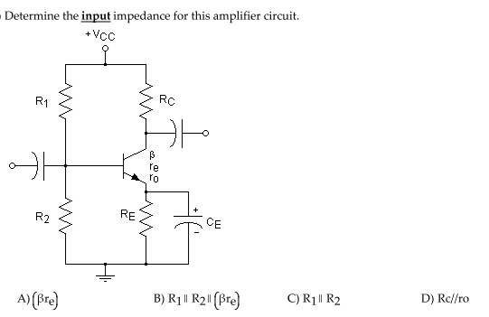
Determine the input impedance for this amplifier circuit. + Vcc RC R1 re ro RE CE R2 D) Rc//ro C) R1|| R2 B) R1 || R2|| (Bre) A) (Bre)


Q: In the compuntation of experimental time constant of an RC circuit in both the charging and…
A: Here it is asked to tell the reason for which we should not directly plot the capacitor voltage as a…
Q: Determine the gradient of the give scalar field V e(2x+3y) cos 5z at R(-0.1, 0.2, 0.4). Select your…
A: The solution is given below
Q: 2VOLTAGE-CURRENT CHARACTERISTICOF A DIODE 1.Explain how to generate the forward-bias portion of the…
A: Solve the problem
Q: Objective 3-Understand the definition and significance of the transfer function; be able to derive a…
A:
Q: 25 V 10 Q Il 12 10 2 13 20 Q
A:
Q: For the network given. Determine Zo. Show solution in your bond paper
A:
Q: Given x[n] = {1000 ,–3,0.1,-1.1,3/4, a}. Determine the value of y[2] if y[n] = x using linear…
A:
Q: 2. For the differential amplifier circuit shown below, calculate the output voltage (including…
A:
Q: If VCC = +18 V, voltage-divider resistor R1 is 4.7 kOhms, and R2 is 1500ohms, then the base bias…
A: The solution is given below
Q: . val 01 Dland D2 1) The PWM is new thechnigue adopted in power electronics application .explaine…
A: Note: We are authorized to answer the first question since the exact one wasn’t specified. Please…
Q: Root loci are usually plotted for variations in the gain. Sometimes we are interested in the…
A:
Q: a) Calculate the wavelength of the radio frequency signal from 980kHz CFPL London b) Calculate the…
A: The solution for first 3 sub-parts have been given in the following sections.
Q: At mid frequencies capacitve elements A) primarily affects low frequency response B) affects both…
A: In this question we will write about bipolar junction transistor related problem answers ....
Q: The capacitor has dielectric constant of e, =100 and conductivity of o=10. Thickness is d=1mm and…
A:
Q: 11. A short circuit test was performed upon a 10kVA, 2300/230V single phase transformer with the…
A: The solution is given below
Q: 49. Use a Karnaugh map to simplify each expression to minimum POS form: (a) (A + B+ C+ D)(A + B + C…
A:
Q: What is a highly doped n semiconductor? What is a doped p semiconductor?
A: What is a highly doped n semiconductor? What is a doped p semiconductor?
Q: A 10kVA single phase transformer designed for 2000/400 V has the following constants, R1 = 5.5 ohms,…
A: The solution is given below
Q: 30 Ω 40 Ω 20 Ω 10 Ω 80 N 60 N 50 Q bo Figure Q2(c)
A:
Q: encoder has 10-bit resolution, is
A: Rotary encoders- The main application of this rotary encoders is monitoring of displacement or…
Q: Q2. Use Delta- star transformation, for the network shown below, to find the equivare resistance…
A:
Q: 11- Consider an analog signal given by s(t) = 2 cos(2n 100t) cos(2n10t) is sampled at the rate of…
A: We need to analyse the signal and sampled signal .
Q: Where is the pn junction? What is n+ region and the p-type substrate?
A:
Q: ng V1 R1 output 2k R2 AC 1 22G R3 3k .ac dec 10 1 10k 1. Determine the value of C so that the cutoff…
A:
Q: 5. An 600 mH inductor and a 3 Q resistor are connected in series with a 1200-V de power supply. a)…
A: Given data, Inductance L = 600 mH Resistance R = 3 ohm Voltage supply V = 1200 V
Q: Find the RMS Voltage and Average Voltage based from the graph
A: It is given that:
Q: 50 SL 20SL %3D O 60 Find Vottay in CI and c리 an Ener Jy and Cz on Ci
A: The solution is given below
Q: (a) Convert points P(1, 3, 5), T(0, -4, 3), and S(-3, -4, -10) from Cartesian to cylindrical and…
A: The solution is given below
Q: A wire has a length of 7.77cm and a cross - sectional area of 7.5 sq.cm. If its resistivity is 0.28…
A: Given: A wire has following specifications l=7.77 cmA=7.5 cm2ρ=0.28 Ωcm
Q: Q2A: A 3-phase induction motor has a star-connected rotor. The rotor e.m.f. at standstill is 50 V.…
A:
Q: Consider the system shown below. We want to sketch the root locus of this system as the parameter a…
A: Note: As per the policy we can solve only 3 sub parts of a question, please re-upload the remaining…
Q: How did they get the equations break down simply?
A: The given voltage transfer characteristics is shown below. A step by step solution is given, we…
Q: (2)Sketch (with straight lines) the frequency response for the function s2 P(S) = (s + 10)4
A:
Q: The no-load current of a transformer is 4A at 0.25 pf when supplied at 25V, 60Hz. Find the…
A:
Q: Explain the exponential relationship between the charge on capacitor and time during charging or…
A: Explanation of exponential relationship between the charge on capacitor and time during charging or…
Q: A voltage of 12 V is applied over a 90m long copper wire that is 4.5 mm in diameter. Estimate the…
A: Given: A copper wire is having Length, l=90 m Diameter, d=4.5 mm Voltage, V=12 V
Q: 13.42 For the circuit in Fig. 13.107, determine the power + absorbed by the 2-N resistor. Assume the…
A: The solution is given below
Q: Use the method of residue to find the inverse Laplace transform of a frequency domain solution given…
A: The solution is given below
Q: Step-1: The first step in constructing a root-locus plot is to locate the open- loop poles and zeros…
A:
Q: For the following System: G(s) = 20 / ( 3s2 + 7 s - 30 ) Compute (Design) a control gain…
A: Steady-state error is the difference between the input and output of the system when it reaches its…
Q: An air-filled copper resonant cavity with dimensions a=19 cm, b=5 cm, c=9 cm, is operated at a…
A:
Q: >> Magnitude Condition: |G(s)H(s)| = 1 >> Rules for Construction of Root Loci Following are the…
A:
Q: Ex. 2170. Refer to Figure 2170. Assume all mks units. Determine Thevenin's and Norton's equivalent…
A:
Q: K sis + )6+2) 0.5
A: We have to draw root locus. we will follow the rules to draw root locus.
Q: the resistors. For example, the current, voltage and power of resistor 1 should be in R1 and so on…
A:
Q: 19 The transfer function of the filter below is: VOUT VIN G = VOUT / VIN V. Vin 1 +1 1000 Vo is: »…
A:
Q: 46. Use the Karnaugh map method to implement the minimum Inputs Output SOP expression for the logic…
A:
Q: 1kVA 230/115 V transformer has been tested for short circuit test and the results are the following:…
A:
Q: Please do problem 2
A:
Q: Q8. A long PN junction cell with area of 2 cm? has the following parameters: Na=lx1019 cm³ Na=3x10¹⁶…
A: PN Junction: The p-n junction is define as an boundary or interface that is present between two…
Kindly choose the best and appropriate answer.

Step by step
Solved in 2 steps with 2 images


- Consider the integrating amplifier circuit in Figure 2. Using nodal analysis, derive an expression for vout for the integrating amplifier. In the circuit in Figure 2, exchange the positions of the 0.1uF capacitor and the 5k resistor. a. Use nodal analysis to generate an expression for vout. b. Using this expression, explain what function this circuit performs on an input signal.How experimental setup is prepared for a CE transistor configuration. Drawits a h-parameter model. Find amplifier parameters given below using this model- (i) Current gain(ii) Input impedance(iii) Voltage Amplification (AVS) consideration source impedance(iv) Current Amplification (AIS) consideration source impedanceSince the transistors used in the circuit are B=100, ro=∞ a) Find the re1, re2 resistance values by performing the DC analysis for each amplifier stage separately. b) Draw the AC equivalent circuit of the amplifier circuit. c)Find the input and output impedance values for each amplifier stage. d) Find the voltage gains AV1, AV2 for each amplifier stage. e) Find the voltage value VL by finding the AV1 Voltage gain.
- Q.4/ Refer to the class AB power amplifier shown below:a. Determine the dc parameters VB(Q1), VB(Q2), ICQ, VCEQ(Q1), VCEQ(Q2).b. For the 5Vrms input, determine the power delivered to the load resistor.c. Determine the approximate input resistance seen by the signal source if ac=100Consider the operational amplifier circuit shown below. Assume the operational amplifier in the circuit is ideal. Determine the expression for the output signal, Vout, in terms of Vin,R1 and R2. Given the expression of the circuit [above’s output signal is Vout =3 − 0.5Vin, what is the maximum and minimum voltage that the input signal can have before the operational amplifier saturates.Amplifier circuit is show below has a single ac input and one ac output. Assuming 2N2222 transistor: 1- Determine the Q point, then illustrate it on the transistor I-V characteristic curves. 2- Is the transistor in the active region? Explain thoroughly. 3- Construct the T-model of the transistor with all parameters labelled and evaluated. Assume room temperature. 4- Draw a complete small signal circuit model, then find the voltage gain. Explain two characteristics of this amplifier. 5- Calculate the current gain, the input resistance, and the output resistance.
- Consider the common-source amplifier shown in Figure P11.50. The NMOS transistor has KP=50 μA/V2, L=5 μm, W=500 μm, Vto=1 V and rd=∞.a. Determine the values of IDQ, VDSQ and gm. b. Compute the voltage gain, input resistance, and output resistance, assuming that the coupling capacitors are short circuits for the ac signal. Repeat Problem P11.50 for an NMOS transistor having KP=50 μA/V2, W=600 μm, L=20 μm, Vto=2 V and rd=∞. Compare the gain with that attained in Problem P11.50.Figure 2 shows a typical BJT amplifier, with its parasitic capacitances displayed. The current gain of the transistor is B=150 and the voltage gain of the amplifier is Am =-125. The small signal resistances of the transistor are re =16 ohm and r0 = infinity, respectively. The values of resistors and capacitors in the figure are: R1 =80 kohm, R2 =20 Kohm, Rc = 2 Kohm, RE = 2 Kohm, Rs =50 W, RI=5 kohm, Cs=2 uF, Cc=2 uF, Ce =10 uF, Cbc =4 pF, Cbe = 10 pF, Cce =1 pF, Cwi = 4 pF, CWO = 9 pF, and Vcc = 20 V. a) Sketch a simplified circuit diagram of Figure 2 for high frequency analysis. b) Using the concept of "Miller effect capacitance", calculate the input and Output Miller effect capacitances of Figure 2, respectively. C) Determine the upper cut-off frequency of Figure 2 that is imposed by its input network only. d) Explain briefly the possible ways to increase the upper cut-off frequencv of this amplifier.The ac equivalent circuit for an amplifier is shown . Assume the capacitors have infinite value, RI = 750 Ω, RB = 100 kΩ, RC = 62 kΩ, and R3 = 100 kΩ. Calculate the voltage gain and input resistance for the amplifier if the BJT Q-point is (40μA, 10 V). Assume βo = 100 and VA = 75V.
- Amplifier circuit is show below has a single ac input and one ac output. Assuming 2N2222 transistor: Construct the T-model of the transistor with all parameters labelled and evaluated. Assume room temperature. Draw a complete small signal circuit model, then find the voltage gain. Explain two characteristics of this amplifier. Calculate the current gain, the input resistance, and the output resistance.According to the circuit in Figure 2:a. Describe the functions of the capacitors in the circuit and their effect on the circuit.b. If the input resistance of RS was added to the amplifier circuit, what would its effect be on the circuit? Please explain.c. Explain the effect of the RL load resistance to be connected to the output of the amplifier circuit after the capacitor on the Circuit's AV strengthening.Derive an expression for the gain Vo/Vs = f(R,△r) by the usage of an ideal operational amplifier model.