Draw the circuit and det (а) Cin (b) Parasitic delay ( (c) Logical effort (g for the following gates. 14-input NAND 2 n-input NAND 3 4-input NOR 4 n-input NOR
Draw the circuit and det (а) Cin (b) Parasitic delay ( (c) Logical effort (g for the following gates. 14-input NAND 2 n-input NAND 3 4-input NOR 4 n-input NOR

Database System Concepts
7th Edition
ISBN:9780078022159
Author:Abraham Silberschatz Professor, Henry F. Korth, S. Sudarshan
Publisher:Abraham Silberschatz Professor, Henry F. Korth, S. Sudarshan
Chapter1: Introduction
Section: Chapter Questions
Problem 1PE

Related questions
Question
please full answer with clear explanition for each step.
Transcribed Image Text:Please do the following problems:
Draw the circuit and determine
(a) Cin
(b) Parasitic delay (P)
(c) Logical effort (g)
for the following gates.
14-input NAND
2 n-input NAND
3 4-input NOR
4 n-input NOR
5 2-input XOR
See Table 4.2 on p. 156 for some final answers.
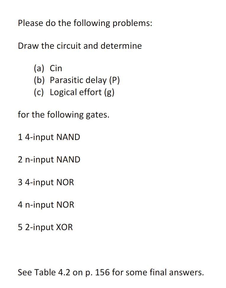
![156
Chapter 4
Delay
4.4.1 Logical Effort
Logical effort of a gate is defined as the ratio of the input capacitance of the gate to the input
capacitance of an inverter that can deliver the same output current. Equivalently, logical effort
indicates how much worse a gate is at producing output current as compared to an
inverter, given that each input of the gate may only present as much input capacitance as
the inverter.
A
Cin = 3
g = 3/3
(a)
Logical effort can be measured in simulation from delay vs. fanout plots as the ratio of
the slope of the delay of the gate to the slope of the delay of an inverter, as will be dis-
cussed in Section 8.5.3. Alternatively, it can be estimated by sketching gates. Figure 4.22
shows inverter, 3-input NAND, and 3-input NOR gates with transistor widths chosen to
achieve unit resistance, assuming PMOS transistors have twice the resistance of nMOS
transistors. The inverter presents three units of input capacitance. The NAND presents
five units of capacitance on each input, so the logical effort is 5/3. Similarly, the NOR pre-
sents seven units of capacitance, so the logical effort is 7/3. This matches our expectation
that NANDS are better than NORS because NORS have slow pMOS transistors in series.
Table 4.2 lists the logical effort of common gates. The effort tends to increase with
the number of inputs. NAND gates are better than NOR gates because the series transis-
tors are nMOS rather than pMOS. Exclusive-OR gates are particularly costly and have
different logical efforts for different inputs. An interesting case is that multiplexers built
from ganged tristates, as shown in Figure 1.29(b), have a logical effort of 2 independent of
the number of inputs. This might at first seem to imply that very large multiplexers are just
as fast as small ones. However, the parasitic delay does increase with multiplexer size;
hence, it is generally fastest to construct large multiplexers out of trees of 4-input multi-
plexers [Sutherland99].
A
C
Cin = 5
g = 5/3
(b)
Y
Cin = 7
g = 7/3
(c)
FIGURE 4.22 Logic gates
sized for unit resistance
TABLE 4.2 Logical effort of common gates
Gate Type
Number of Inputs
4
n
inverter
1
NAND
4/3
5/3
6/3
(n + 2)/3
NOR
5/3
7/3
9/3
(2n + 1)/3
tristate, multiplexer
2
XOR, XNOR
4, 4
6, 12, 6
8, 16, 16, 8
4.4.2 Parasitic Delay
The parasitic delay of a gate is the delay of the gate when it drives zero load. It can be esti-
mated with RC delay models. A crude method good for hand calculations is to count only
diffusion capacitance on the output node. For example, consider the gates in Figure 4.22,
assuming each transistor on the output node has its own drain diffusion contact. Transis-
tor widths were chosen to give a resistance of R in each gate. The inverter has three units
of diffusion capacitance on the output, so the parasitic delay is 3RC = t. In other words,
SThis assumption is made throughout the book. Exercises 4.19-4.20 explore the effects of different relative
resistances (see also [Sutherland99]). The overall conclusions do not change very much, so the simple
model is good enough for most hand estimates. A simulator or static timing analyzer should be used when
more accurate results are required.
ABC](/v2/_next/image?url=https%3A%2F%2Fcontent.bartleby.com%2Fqna-images%2Fquestion%2F02d4a278-05d2-46c7-a876-b876648b6b8a%2Fad4ef4b0-f7b7-430c-9798-b83d870ee69f%2Fytt8rl_processed.jpeg&w=3840&q=75)
Transcribed Image Text:156
Chapter 4
Delay
4.4.1 Logical Effort
Logical effort of a gate is defined as the ratio of the input capacitance of the gate to the input
capacitance of an inverter that can deliver the same output current. Equivalently, logical effort
indicates how much worse a gate is at producing output current as compared to an
inverter, given that each input of the gate may only present as much input capacitance as
the inverter.
A
Cin = 3
g = 3/3
(a)
Logical effort can be measured in simulation from delay vs. fanout plots as the ratio of
the slope of the delay of the gate to the slope of the delay of an inverter, as will be dis-
cussed in Section 8.5.3. Alternatively, it can be estimated by sketching gates. Figure 4.22
shows inverter, 3-input NAND, and 3-input NOR gates with transistor widths chosen to
achieve unit resistance, assuming PMOS transistors have twice the resistance of nMOS
transistors. The inverter presents three units of input capacitance. The NAND presents
five units of capacitance on each input, so the logical effort is 5/3. Similarly, the NOR pre-
sents seven units of capacitance, so the logical effort is 7/3. This matches our expectation
that NANDS are better than NORS because NORS have slow pMOS transistors in series.
Table 4.2 lists the logical effort of common gates. The effort tends to increase with
the number of inputs. NAND gates are better than NOR gates because the series transis-
tors are nMOS rather than pMOS. Exclusive-OR gates are particularly costly and have
different logical efforts for different inputs. An interesting case is that multiplexers built
from ganged tristates, as shown in Figure 1.29(b), have a logical effort of 2 independent of
the number of inputs. This might at first seem to imply that very large multiplexers are just
as fast as small ones. However, the parasitic delay does increase with multiplexer size;
hence, it is generally fastest to construct large multiplexers out of trees of 4-input multi-
plexers [Sutherland99].
A
C
Cin = 5
g = 5/3
(b)
Y
Cin = 7
g = 7/3
(c)
FIGURE 4.22 Logic gates
sized for unit resistance
TABLE 4.2 Logical effort of common gates
Gate Type
Number of Inputs
4
n
inverter
1
NAND
4/3
5/3
6/3
(n + 2)/3
NOR
5/3
7/3
9/3
(2n + 1)/3
tristate, multiplexer
2
XOR, XNOR
4, 4
6, 12, 6
8, 16, 16, 8
4.4.2 Parasitic Delay
The parasitic delay of a gate is the delay of the gate when it drives zero load. It can be esti-
mated with RC delay models. A crude method good for hand calculations is to count only
diffusion capacitance on the output node. For example, consider the gates in Figure 4.22,
assuming each transistor on the output node has its own drain diffusion contact. Transis-
tor widths were chosen to give a resistance of R in each gate. The inverter has three units
of diffusion capacitance on the output, so the parasitic delay is 3RC = t. In other words,
SThis assumption is made throughout the book. Exercises 4.19-4.20 explore the effects of different relative
resistances (see also [Sutherland99]). The overall conclusions do not change very much, so the simple
model is good enough for most hand estimates. A simulator or static timing analyzer should be used when
more accurate results are required.
ABC
Expert Solution
This question has been solved!
Explore an expertly crafted, step-by-step solution for a thorough understanding of key concepts.

This is a popular solution!

Trending now
This is a popular solution!

Step by step
Solved in 5 steps with 5 images

Knowledge Booster


Learn more about
Need a deep-dive on the concept behind this application? Look no further. Learn more about this topic, computer-science and related others by exploring similar questions and additional content below.Recommended textbooks for you
Database System Concepts
Computer Science
ISBN:
9780078022159
Author:
Abraham Silberschatz Professor, Henry F. Korth, S. Sudarshan
Publisher:
McGraw-Hill Education

Starting Out with Python (4th Edition)
Computer Science
ISBN:
9780134444321
Author:
Tony Gaddis
Publisher:
PEARSON

Digital Fundamentals (11th Edition)
Computer Science
ISBN:
9780132737968
Author:
Thomas L. Floyd
Publisher:
PEARSON
Database System Concepts
Computer Science
ISBN:
9780078022159
Author:
Abraham Silberschatz Professor, Henry F. Korth, S. Sudarshan
Publisher:
McGraw-Hill Education
Starting Out with Python (4th Edition)
Computer Science
ISBN:
9780134444321
Author:
Tony Gaddis
Publisher:
PEARSON
Digital Fundamentals (11th Edition)
Computer Science
ISBN:
9780132737968
Author:
Thomas L. Floyd
Publisher:
PEARSON

C How to Program (8th Edition)
Computer Science
ISBN:
9780133976892
Author:
Paul J. Deitel, Harvey Deitel
Publisher:
PEARSON

Database Systems: Design, Implementation, & Manag…
Computer Science
ISBN:
9781337627900
Author:
Carlos Coronel, Steven Morris
Publisher:
Cengage Learning

Programmable Logic Controllers
Computer Science
ISBN:
9780073373843
Author:
Frank D. Petruzella
Publisher:
McGraw-Hill Education