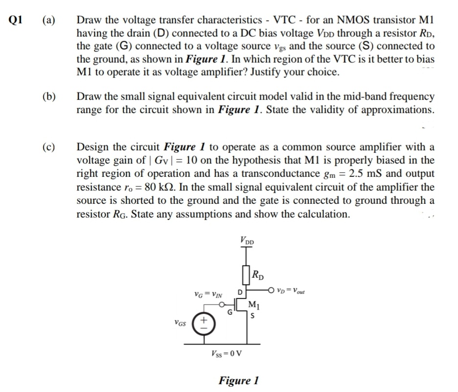
Draw the voltage transfer characteristics VTC - for an NMOS transistor M1 having the drain (D) connected to a DC bias voltage VDD through a resistor Rp, the gate (G) connected to a voltage source vgs and the source (S) connected to the ground, as shown in Figure 1. In which region of the VTC is it better to bias M1 to operate it as voltage amplifier? Justify your choice. Q1 (a) (b) Draw the small signal equivalent circuit model valid in the mid-band frequency range for the circuit shown in Figure 1. State the validity of approximations. Design the circuit Figure 1 to operate as a common source amplifier with a voltage gain of | Gv| = 10 on the hypothesis that M1 is properly biased in the right region of operation and has a transconductance gm = 2.5 mS and output resistance ro = 80 k2. In the small signal equivalent circuit of the amplifier the source is shorted to the ground and the gate is connected to ground through a resistor RG. State any assumptions and show the calculation. (c) VDD Rp Vp=Vout VG = VIN M1 VGS Vss=0 V Figure 1
Draw the voltage transfer characteristics VTC - for an NMOS transistor M1 having the drain (D) connected to a DC bias voltage VDD through a resistor Rp, the gate (G) connected to a voltage source vgs and the source (S) connected to the ground, as shown in Figure 1. In which region of the VTC is it better to bias M1 to operate it as voltage amplifier? Justify your choice. Q1 (a) (b) Draw the small signal equivalent circuit model valid in the mid-band frequency range for the circuit shown in Figure 1. State the validity of approximations. Design the circuit Figure 1 to operate as a common source amplifier with a voltage gain of | Gv| = 10 on the hypothesis that M1 is properly biased in the right region of operation and has a transconductance gm = 2.5 mS and output resistance ro = 80 k2. In the small signal equivalent circuit of the amplifier the source is shorted to the ground and the gate is connected to ground through a resistor RG. State any assumptions and show the calculation. (c) VDD Rp Vp=Vout VG = VIN M1 VGS Vss=0 V Figure 1

Introductory Circuit Analysis (13th Edition)
13th Edition
ISBN:9780133923605
Author:Robert L. Boylestad
Publisher:Robert L. Boylestad
Chapter1: Introduction
Section: Chapter Questions
Problem 1P: Visit your local library (at school or home) and describe the extent to which it provides literature...

Related questions
Question
Transcribed Image Text:Draw the voltage transfer characteristics VTC - for an NMOS transistor M1
having the drain (D) connected to a DC bias voltage VDD through a resistor RD,
the gate (G) connected to a voltage source vgs and the source (S) connected to
the ground, as shown in Figure 1. In which region of the VTC is it better to bias
M1 to operate it as voltage amplifier? Justify your choice.
Q1
(a)
(b)
Draw the small signal equivalent circuit model valid in the mid-band frequency
range for the circuit shown in Figure 1. State the validity of approximations.
Design the circuit Figure 1 to operate as a common source amplifier with a
voltage gain of | Gv|= 10 on the hypothesis that M1 is properly biased in the
right region of operation and has a transconductance gm = 2.5 mS and output
resistance ro = 80 kN. In the small signal equivalent circuit of the amplifier the
source is shorted to the ground and the gate is connected to ground through a
resistor RG. State any assumptions and show the calculation.
(c)
VDD
Rp
O vD=Vout
VG = VIN
M1
G
VGS
Vss =0 V
Figure 1
Expert Solution
This question has been solved!
Explore an expertly crafted, step-by-step solution for a thorough understanding of key concepts.

This is a popular solution!

Trending now
This is a popular solution!

Step by step
Solved in 3 steps with 1 images

Knowledge Booster


Learn more about
Need a deep-dive on the concept behind this application? Look no further. Learn more about this topic, electrical-engineering and related others by exploring similar questions and additional content below.Recommended textbooks for you
Introductory Circuit Analysis (13th Edition)
Electrical Engineering
ISBN:
9780133923605
Author:
Robert L. Boylestad
Publisher:
PEARSON

Delmar's Standard Textbook Of Electricity
Electrical Engineering
ISBN:
9781337900348
Author:
Stephen L. Herman
Publisher:
Cengage Learning

Programmable Logic Controllers
Electrical Engineering
ISBN:
9780073373843
Author:
Frank D. Petruzella
Publisher:
McGraw-Hill Education
Introductory Circuit Analysis (13th Edition)
Electrical Engineering
ISBN:
9780133923605
Author:
Robert L. Boylestad
Publisher:
PEARSON
Delmar's Standard Textbook Of Electricity
Electrical Engineering
ISBN:
9781337900348
Author:
Stephen L. Herman
Publisher:
Cengage Learning
Programmable Logic Controllers
Electrical Engineering
ISBN:
9780073373843
Author:
Frank D. Petruzella
Publisher:
McGraw-Hill Education

Fundamentals of Electric Circuits
Electrical Engineering
ISBN:
9780078028229
Author:
Charles K Alexander, Matthew Sadiku
Publisher:
McGraw-Hill Education

Electric Circuits. (11th Edition)
Electrical Engineering
ISBN:
9780134746968
Author:
James W. Nilsson, Susan Riedel
Publisher:
PEARSON

Engineering Electromagnetics
Electrical Engineering
ISBN:
9780078028151
Author:
Hayt, William H. (william Hart), Jr, BUCK, John A.
Publisher:
Mcgraw-hill Education,