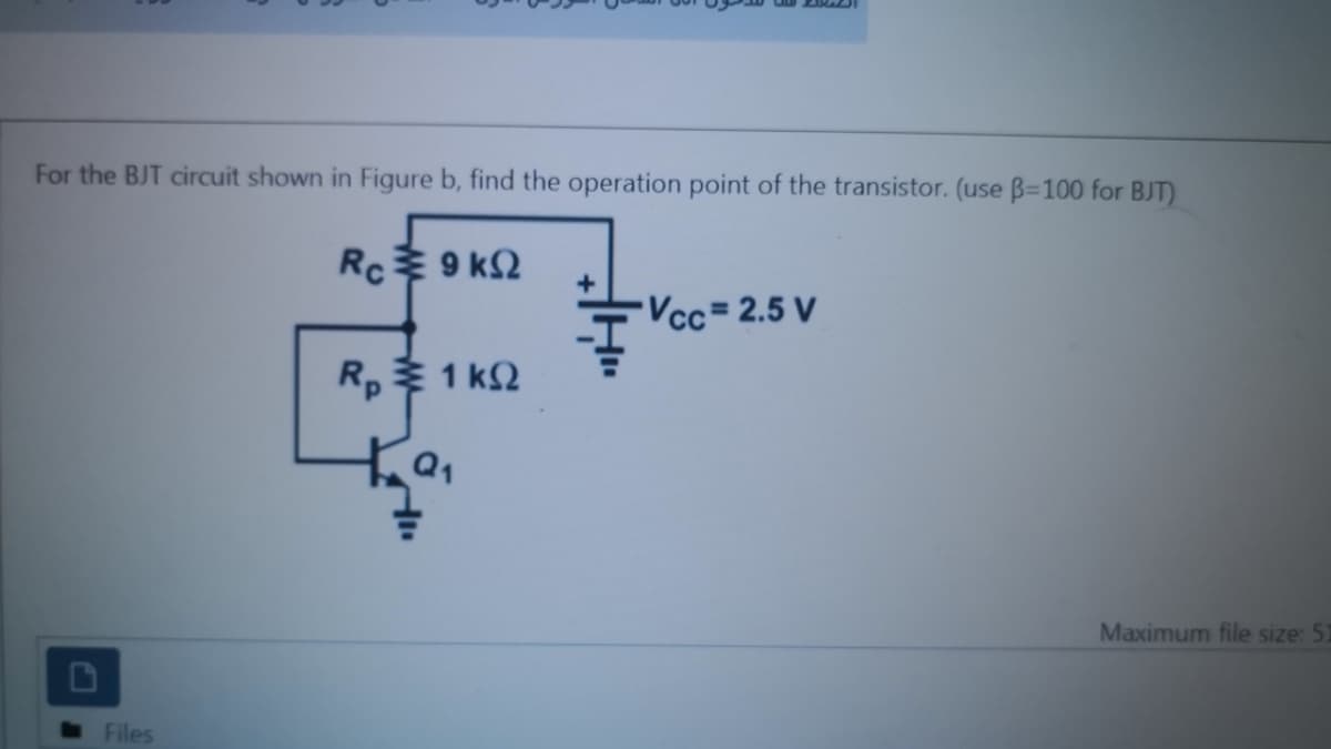
For the BJT circuit shown in Figure b, find the operation point of the transistor. (use B=100 for BJT) Rc 9 k2 Vcc= 2.5 V R, 1 k2 Q1


Q: with a voltage divider bias below and with the following values: Rc, RE = 100 N, Vcc = 10 V,…
A: Here it is assumed that the transistor is in active region as per the question. We have applied KVL…
Q: 16 CONSIDER A TWO-BJT CONFIGURATION IN PIGURE 1. you MAY ASSUME THAT BOTH TRANSISTORS ARE THE SAME…
A: BJT and MOSFET are the class of transistors used in analog electronics. They are widely used…
Q: From the give two-BJT configuration in Figure 1. You may assume that both transistors are the same…
A:
Q: Vin For the circuit shown, assume that Vo = 3V and that the transistor is described as follows: Kn =…
A: For the above given question we need to perform AC and DC analysis of the given amplifier.
Q: In a CE transistor, Vcc=12 V and the zero signal collector current is 1mA. Determine the operating…
A: Given: CE transistor Vcc=12 VIc=1 mARc=6 Ω
Q: Solve this: Transistor AC Analysis a. Determine the re b. Calculate the Vb and Vc c. Determine…
A: The required parameters can be calculated by using the DC and AC analysis of the amplifier circuit.
Q: How: For the fixed bias BJT circuit B = VCE IC, RL=8 and vcc = 24 V; determine the maximum Power…
A: Given, Configuration - fixed bias RL = 8 ohm Vcc = 24 volts
Q: BO + Q1 VCE VBE Q2 E
A: We will find out the DC current gain for given circuit
Q: A pnp transistor with ß = 60 is connected in a common-base configuration as shown in Figure below.…
A:
Q: A BJT diff-amp circuit
A: BJT (bipolar junction transistor)A transistor having a three terminal made up of semiconductor…
Q: Consider the common-base BJT amplifier in Figure 7. Assume that the following values remain constant…
A: Dear student as per our guidelines we are supposed to solve only one question in which it should be…
Q: Q: For the circuit shown draw the ac equivalent circuit and find Avs, Ai, Zi and Zo, where hie=1k2,…
A: "According to the Company's policy, we will provide solution of first three parts of the question ,…
Q: 1- If you have the following Q-point specifications VCB=6V Ic=1.4 mA IB = 10 μA Av=186 R₁ = 22K0 For…
A: “Since you have posted a question with multiple sub-parts, we will solve first three sub-parts for…
Q: For the circuit shown in Figure 2 let Vcc=5 V, R₂ = 4 kQ2, Re = 3 k2, R₁ = 60 k2, and R₂ = 40 k2.…
A: We are authorized to answer three subparts at a time, since you have not mentioned which part you…
Q: C IDER A TWO- BJT CONFIGURATION IN FIGURE 1. You ASSUME THAT BOTH TRANSISTORS ARE THE SAME WITH SAME…
A:
Q: BO + Q1 CE VBE Q2 +
A:
Q: A common-emitter circuit using a BJT transistor (Figure 2a) is used to turn on a resistive load R2 =…
A:
Q: Consider a two-BJT configuration in Figure 1. You may assume that both transistors are the same with…
A: We need to find out the voltage to on transistor , then we will find dc current Gain .
Q: 4) In the figure below, C1 and C2 are very large. Determine the following (a) Quiescent collector…
A: Brief description: For the above given common emitter PNP transistor circuit we need to calculate…
Q: From the transistor collector characteristic shown, determine βac for an operating point of IB =…
A: From the Question From the transistor collector characteristic shown, determine βac for an operating…
Q: Design the bias circuit to give aQ-point of IC = 20 μA and VC E = 0.90 V ifthe transistor current…
A: Concept: A semiconductor device used to amplify or switch electronic signals and electrical power is…
Q: Using the BJT small-signal model given in Figure 2, determine the AC current gain A = iout/in for…
A: As per our company guidelines we are supposed to answer only first question kindly repost other…
Q: Ex 3.21: For the p-channel transistor in the circuit in Figure, the parameters are: Inss = 6 mA, Vr=…
A: Transistor: A transistor is a device that controls current or voltage flow and serves as an…
Q: 2.Consider one Design/Circuit of MOSFET (can be as a small signal amplifier and digital switches)…
A: 2. Consider one Design/Circuit of MOSFET ;
Q: In a side-transistor circuit The maximum values are given below. Normal maximum VCC voltage of the…
A: Explanation: Given that, Ic(max) = 100 mA, Vce(max) = 20 volt Now,
Q: Fundamentals of BJT) Determine: a) Transistor terminal voltages b) Transistor junction voltages
A: Brief description : Here in the question they have mentioned a PNP transistor circuit. In case of…
Q: 20x lo Rc 50 ohm Vcc = 10V Vg = 0.8 V Calculate the lc for Qi. Show that Q1 is in Forward Active…
A: NOTE: Since you have asked multiple questions, we will solve the first question for you. If you want…
Q: Consider a two-BJT configuration in Figure 1. You may assume that both transistors are the same with…
A:
Q: For the BJT amplifier below, VCEQ = 6.12 V, Ico = 3.05mA, RE = 910 2, Vcc = 15 V, B of the Si…
A:
Q: For the circuit in figure 2. VDD = 5 V. The threshold voltage of the N-MOS transistor is VT = 1 V.…
A: From Given figure IB=0--0.710k=70μAwhereas, IC=βIB=200×70μA=14mAWe can write,VG=5-IC(470)=-1.58Vwe…
Q: A pnp transistor with ß = 60 is connected in a common-base configuration as shown in Figure below.…
A:
Q: Determine the value of IB, Ic and VCE for the base-biased transistor circuit in figure belov with…
A: Given circuit Given parameters: VCC=12 VβDC=90RB=22 KΩRC=100 Ω
Q: A constant-current source is shown in Figure (Q1), the BJI information is: • B = 100 • V = 100 V •…
A: Common emitter Configuration- Common emitter configuration-Emitter is common between input and…
Q: circuit components. A three-input CML XOR gate using BJTS (bipolar junction transistors) is shown…
A: In this question we will write about list of electrical circuit components....
Q: Ic 3302 RC IB Vcc 20V 47 k2 VBE VBB 10V IE
A: We need to find out the current and voltage for given circuit .
Q: Q1) Design the bias of MOSFET such that the Q-point is in middle of saturation region. Assume Vtn…
A: MOSFET: A Metal–Oxide–Semiconductor Field-Effect Transistor (MOSFET) is a field-effect transistor…
Q: 2021H (a) Plot the output characteristics of the transistor (b) Draw the DC load line (c) Determine…
A:
Q: Exercise 1: In a transistor, collector load is Rc = 3 KQ whereas quiescent current (zero signal…
A:
Q: How to use bjt to control mosfet as a switch with detailed circuit diagram
A: Bipolar junction transistor is act as a switch if it operates in cutoff and saturation mode of its…
Q: For each transistor shown in Figure P10.1,determine whether the BE and BC junctions areforward- or…
A: (a) Given transistor is – From figure – It is a pnp transistor. Value of voltage VBE = -0.6V and…
Q: For the circuit in Figure 1, the transistor is biased so that ICQ is 10 mA and VCEQ is 8 V. As a…
A: Given information: ICQ=10 mA=10×10-3A. VCEQ=8 Volt. These values for collector current and collector…
Q: If the common base DC current gain (a) of a BJT is 0.95, its common emitter DC current gain is
A:
Q: transistor is biased
A: Bipolar Junction Transistor (BJT)- This kind of transistor uses both electrons and holes as charge…
Q: 2. A load of 8Ω is supplied by a single-switch Direct Current (DC) chopper with an input voltage of…
A:
Q: |12.5 The class A emitter follower in the figure to the right is to operate from +/- 10 V supplies…
A: The problem can be solved in the following way: Let the current gain of the transistor is infinite.…
Q: VEB Ic = Ise r . Assume that the PNP transistor is in the forward active region. Round the answers…
A:
Q: Design a common emitter transistor so that it will operate in the linear region with a max swing on…
A: The collector to emitter voltage is given by:
Q: For the circut below measurement indicates that Vb = -1.5V. a) Assuming Vbe=0.7, calculate Ve,α,β…
A: With the help of given base voltage Vb = -1.5 V We calculated the base current and from the…
Q: The fixed-bias circuit of Figure 1 (a) is the simplest transistor dc bias configuration. The…
A:
Q: Q#1: Explain Bipolar Junction Transistor (BJT) also explain how BJT work as an Amplifier.
A: Introduction: A bipolar junction transistor, or BJT, is a solid-state device in which the amount of…

Step by step
Solved in 4 steps with 1 images


- The dc load line on a family of collector characteristic curves of transistor shows the........ Choose correct answer : A) All operating regions B) cut-off region only C) active region only D) saturation region onlyWhat is the collector-emitter voltage for thetransistor if IS = 7 × 10⁻¹⁶ μA,αF = 0.99, and αR = 0.5? (b) What is the emittercollector voltage for the transistor P5.56(b)for the same transistor parameters?Draw an NPN transistor Circuit with Vbb = 3V, Rb = 23k Ohms, Vcc = 10 V, Rc = 800 Ohms, Beta = 30. Determine Loadline, Vce = ?, Ic =?, mkde of operation. Please show all work. I will definately rate. Thank you!
- The maximum drain current for the n-channel enrichment type MOSFET is 30 mA.Determine VGS with this current level if k= 0.06x10⁻³ A/V2 and VT is the maximum value.I need answer ASAP. Thank you! A.) Find the value of drain current and gate current. B.) What type of JFET DC biasing is this? C.) Find the Drain voltage, Emitter Voltage and Gate VoltageDefine the type of transistors and the region of operation (cut-off, linear, saturation) for each transistor. Assume Vdd = 3.3V and thresholds VTn = |VTp| = 1.4V . VDSATn = |VDSATp| = 1.0V . Explain your answer. PART D PLEASE
- Q.1 (a) (i) State three differences between the Field Effect Transistor (FET) and the Bipolar Junction Transistor (BJT). (ii) Draw the physical structure and device symbol for an n-channel JFET. (iii) What is meant by drain characteristicsQuestion : The current in an enchcement mode NMOS transistor bised in saturation mode was measured to be 1 mA at a drain source voltage of 5v . when the drain source voltage was increased to 6v while keeping gate source voltage same. The drain current increase to 1.02 mA.Assume that drain to source saturation voltage is much smaller than the aaplied drain source voltage . the channel length modulation parameter λ(in v-1)isQues 4: Draw the structure of an N-channel JFET and also explain the drain characteristics
- Determine the output currents and voltage of the Transistor Ic, IB, VCE. Beta= 120, Vbe = 0.7v.An n-channel JFET has a drain-source saturation current IDSS = 10 mA and a gate-source pinch-off voltage of -4 volts. If the drain current is 2.5 mA, calculate the gate-source voltage, VGS.15/ In a transistor, _____________________________________________ is the process of making proper flow of zero signal collector current and the maintenance of proper collector-emitter voltage during the passage of signal. a. DC load line drawing b. amplification c. transistor biasing d. stabilization