For the circuit shown in the adjacent figure: a) What type of biasing shown in figure? b) Determine Ic c) Determine VB and Vc. d) What is value of Rc that can be used to decrease Ic by 25 percent? +3V RC 33 kN Boc
For the circuit shown in the adjacent figure: a) What type of biasing shown in figure? b) Determine Ic c) Determine VB and Vc. d) What is value of Rc that can be used to decrease Ic by 25 percent? +3V RC 33 kN Boc

Delmar's Standard Textbook Of Electricity
7th Edition
ISBN:9781337900348
Author:Stephen L. Herman
Publisher:Stephen L. Herman
Chapter30: Dc Motors
Section: Chapter Questions
Problem 6RQ: What is CEMF?

Related questions
Question
electric , please solve question a and b
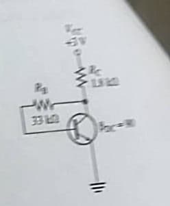
Transcribed Image Text:Wr
33 L0
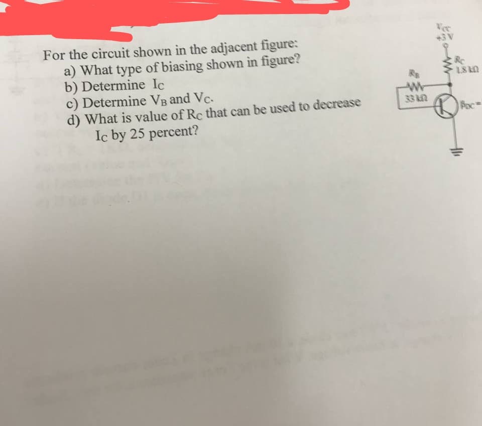
Transcribed Image Text:Vec
+3V
For the circuit shown in the adjacent figure:
a) What type of biasing shown in figure?
b) Determine Ic
c) Determine VB and Vc.
d) What is value of Rc that can be used to decrease
Ic by 25 percent?
RC
1.8 KO
Wr
33 kn
Boc
Expert Solution
This question has been solved!
Explore an expertly crafted, step-by-step solution for a thorough understanding of key concepts.

Step by step
Solved in 4 steps with 4 images

Knowledge Booster


Learn more about
Need a deep-dive on the concept behind this application? Look no further. Learn more about this topic, electrical-engineering and related others by exploring similar questions and additional content below.Recommended textbooks for you
Delmar's Standard Textbook Of Electricity
Electrical Engineering
ISBN:
9781337900348
Author:
Stephen L. Herman
Publisher:
Cengage Learning
Delmar's Standard Textbook Of Electricity
Electrical Engineering
ISBN:
9781337900348
Author:
Stephen L. Herman
Publisher:
Cengage Learning