For the transistor feedback amplifier shown, hg = 100, hje = 1 K, hre = 0 %3D and hoe = 0. Determine V where 1, R, a) A b) Agf c) Rf d) Rf %3D Vcc 10 K 100 K ww R' V. R = 1K Rot ww-
For the transistor feedback amplifier shown, hg = 100, hje = 1 K, hre = 0 %3D and hoe = 0. Determine V where 1, R, a) A b) Agf c) Rf d) Rf %3D Vcc 10 K 100 K ww R' V. R = 1K Rot ww-

Power System Analysis and Design (MindTap Course List)
6th Edition
ISBN:9781305632134
Author:J. Duncan Glover, Thomas Overbye, Mulukutla S. Sarma
Publisher:J. Duncan Glover, Thomas Overbye, Mulukutla S. Sarma
Chapter12: Power System Controls
Section: Chapter Questions
Problem 12.3P

Related questions
Question
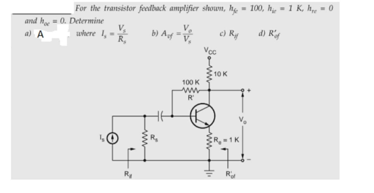
Transcribed Image Text:= 100, h = 1 K, h,e = 0
%3D
For the transistor feedback amplifier shown, hg.
and h = 0. Determine
where 1,=
Ve
b) Af =V
c) Rf
d) Rf
a) A
%3D
R,
Vcc
10 K
100 K
R'
R = 1 K
Rit
Rof
ww
Expert Solution
This question has been solved!
Explore an expertly crafted, step-by-step solution for a thorough understanding of key concepts.

Step by step
Solved in 2 steps

Knowledge Booster


Learn more about
Need a deep-dive on the concept behind this application? Look no further. Learn more about this topic, electrical-engineering and related others by exploring similar questions and additional content below.Recommended textbooks for you
Power System Analysis and Design (MindTap Course …
Electrical Engineering
ISBN:
9781305632134
Author:
J. Duncan Glover, Thomas Overbye, Mulukutla S. Sarma
Publisher:
Cengage Learning
Power System Analysis and Design (MindTap Course …
Electrical Engineering
ISBN:
9781305632134
Author:
J. Duncan Glover, Thomas Overbye, Mulukutla S. Sarma
Publisher:
Cengage Learning