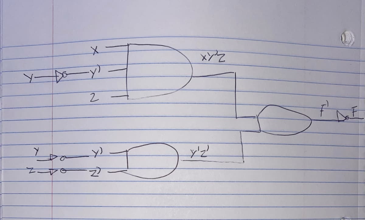
I need the drawing of the circuit. "convert the SOP (AND/OR) circuit diagram into one containing only NAND and NOR gates." I have included the picture of the SOP Circuit that needs to be converted. Please draw the circuit clearly and answer question 1 completly
I need the drawing of the circuit. "convert the SOP (AND/OR) circuit diagram into one containing only NAND and NOR gates." I have included the picture of the SOP Circuit that needs to be converted. Please draw the circuit clearly and answer question 1 completly

Introductory Circuit Analysis (13th Edition)
13th Edition
ISBN:9780133923605
Author:Robert L. Boylestad
Publisher:Robert L. Boylestad
Chapter1: Introduction
Section: Chapter Questions
Problem 1P: Visit your local library (at school or home) and describe the extent to which it provides literature...

Related questions
Question
I need the drawing of the circuit. "convert the SOP (AND/OR) circuit diagram into one containing only NAND and NOR gates."
I have included the picture of the SOP Circuit that needs to be converted. Please draw the circuit clearly and answer question 1 completly, thanks...
quick response gets thumbs up
Transcribed Image Text:xンZ
ソー
(人
![Here you will not build a circuit--only draw its diagram (using ExpressSCH). In Exp #6.2, you chose a function F (X, Y, Z) and designed the
circuit using ANDS, ORS, and inverters in SOP and POS form. For this section, convert the SOP (AND/OR) circuit diagram (the one you did not
build) into one containing only NAND and NOR gates. (Do not use NOT gates; a NOR or NAND will serve as a NOT if you tie all its inputs
together.)
Use DM (DeMorgan) equivalent gate symbols where they are needed, but only then. DM symbols have their inverter bubbles at the front, so
use them if their inputs come from gates with bubbled outputs (NORMAL symbols) or from external inputs that are inverted (e.g. x). Otherwise,
do not use them. The point is that connecting wires should either have a bubble at each end so the bubbles cancel, O 0, or no
bubbles at all (see diagrams in [Slide 1. SOP Circuit and NAND/NOR Circuit],).
Since NANDS are just bubbled ANDS and NORS are just bubbled ORs, your NAND/NOR circuit should resemble the AND/OR design of Exp
#6.2, And that is the point; if the connecting wires are bubbled at each end, you can ignore the bubbles and see circuit logic as easily as in
Exp#6.2.
Also, in converting to a NAND/NOR circuit, you might be able to replace two OR gates with a 3-input invert-OR. Example: to produce the OR
expression x + Y + Z, use the 3-input NAND (7410) drawn as an invert OR (notice the inputs have been inverted).
X-
O 7410
In your lab notebook, include the SOP equation for F and its corresponding circuit diagram from Exp #6.2 as well as the circuit diagram created
here. Remember to use DeMorgan gate symbols but only where they are needed. If you use only normal symbols throughout, it will not be
possible to follow circuit logic simply by looking at the diagram.
Question
1. How many chips (not gates) were required in the circuit of Exp #6.2 compared to the number required here? Did using NANDS and NORS
reduce the number of chips?
IX >IN](/v2/_next/image?url=https%3A%2F%2Fcontent.bartleby.com%2Fqna-images%2Fquestion%2F2aae8944-2a4b-4fda-bc7f-e672aabc9087%2Ffd020b07-5756-4b06-b5df-6e8e351cf0d2%2F61xtgf9_processed.jpeg&w=3840&q=75)
Transcribed Image Text:Here you will not build a circuit--only draw its diagram (using ExpressSCH). In Exp #6.2, you chose a function F (X, Y, Z) and designed the
circuit using ANDS, ORS, and inverters in SOP and POS form. For this section, convert the SOP (AND/OR) circuit diagram (the one you did not
build) into one containing only NAND and NOR gates. (Do not use NOT gates; a NOR or NAND will serve as a NOT if you tie all its inputs
together.)
Use DM (DeMorgan) equivalent gate symbols where they are needed, but only then. DM symbols have their inverter bubbles at the front, so
use them if their inputs come from gates with bubbled outputs (NORMAL symbols) or from external inputs that are inverted (e.g. x). Otherwise,
do not use them. The point is that connecting wires should either have a bubble at each end so the bubbles cancel, O 0, or no
bubbles at all (see diagrams in [Slide 1. SOP Circuit and NAND/NOR Circuit],).
Since NANDS are just bubbled ANDS and NORS are just bubbled ORs, your NAND/NOR circuit should resemble the AND/OR design of Exp
#6.2, And that is the point; if the connecting wires are bubbled at each end, you can ignore the bubbles and see circuit logic as easily as in
Exp#6.2.
Also, in converting to a NAND/NOR circuit, you might be able to replace two OR gates with a 3-input invert-OR. Example: to produce the OR
expression x + Y + Z, use the 3-input NAND (7410) drawn as an invert OR (notice the inputs have been inverted).
X-
O 7410
In your lab notebook, include the SOP equation for F and its corresponding circuit diagram from Exp #6.2 as well as the circuit diagram created
here. Remember to use DeMorgan gate symbols but only where they are needed. If you use only normal symbols throughout, it will not be
possible to follow circuit logic simply by looking at the diagram.
Question
1. How many chips (not gates) were required in the circuit of Exp #6.2 compared to the number required here? Did using NANDS and NORS
reduce the number of chips?
IX >IN
Expert Solution
This question has been solved!
Explore an expertly crafted, step-by-step solution for a thorough understanding of key concepts.

This is a popular solution!

Trending now
This is a popular solution!

Step by step
Solved in 2 steps with 2 images

Knowledge Booster


Learn more about
Need a deep-dive on the concept behind this application? Look no further. Learn more about this topic, electrical-engineering and related others by exploring similar questions and additional content below.Recommended textbooks for you
Introductory Circuit Analysis (13th Edition)
Electrical Engineering
ISBN:
9780133923605
Author:
Robert L. Boylestad
Publisher:
PEARSON

Delmar's Standard Textbook Of Electricity
Electrical Engineering
ISBN:
9781337900348
Author:
Stephen L. Herman
Publisher:
Cengage Learning

Programmable Logic Controllers
Electrical Engineering
ISBN:
9780073373843
Author:
Frank D. Petruzella
Publisher:
McGraw-Hill Education
Introductory Circuit Analysis (13th Edition)
Electrical Engineering
ISBN:
9780133923605
Author:
Robert L. Boylestad
Publisher:
PEARSON
Delmar's Standard Textbook Of Electricity
Electrical Engineering
ISBN:
9781337900348
Author:
Stephen L. Herman
Publisher:
Cengage Learning
Programmable Logic Controllers
Electrical Engineering
ISBN:
9780073373843
Author:
Frank D. Petruzella
Publisher:
McGraw-Hill Education

Fundamentals of Electric Circuits
Electrical Engineering
ISBN:
9780078028229
Author:
Charles K Alexander, Matthew Sadiku
Publisher:
McGraw-Hill Education

Electric Circuits. (11th Edition)
Electrical Engineering
ISBN:
9780134746968
Author:
James W. Nilsson, Susan Riedel
Publisher:
PEARSON

Engineering Electromagnetics
Electrical Engineering
ISBN:
9780078028151
Author:
Hayt, William H. (william Hart), Jr, BUCK, John A.
Publisher:
Mcgraw-hill Education,