if a QAM modulated signal is Q mtlcoswet+mSincwet and Find out the massage signal.
if a QAM modulated signal is Q mtlcoswet+mSincwet and Find out the massage signal.

Chapter22: Sequence Control
Section: Chapter Questions
Problem 6SQ: Draw a symbol for a solid-state logic element AND.

Related questions
Question
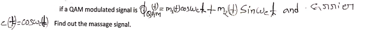
Transcribed Image Text:if a QAM modulated signal is
Pa mtdeswettm) Sinwet and Ginnien
Find out the massage signal.
Expert Solution
This question has been solved!
Explore an expertly crafted, step-by-step solution for a thorough understanding of key concepts.

Step by step
Solved in 2 steps with 1 images

Knowledge Booster


Learn more about
Need a deep-dive on the concept behind this application? Look no further. Learn more about this topic, electrical-engineering and related others by exploring similar questions and additional content below.Recommended textbooks for you

Delmar's Standard Textbook Of Electricity
Electrical Engineering
ISBN:
9781337900348
Author:
Stephen L. Herman
Publisher:
Cengage Learning
Delmar's Standard Textbook Of Electricity
Electrical Engineering
ISBN:
9781337900348
Author:
Stephen L. Herman
Publisher:
Cengage Learning