II. Attach C to B, forming a BJT. A. Identify the type of BJT (NPN or PNP). Where is the emitter, base and the collector? B -_ C- Answer with A - B. In forward active mode, why does a large current flow in the base-collector junction, even though it's reverse-biased? Answer in 1 sentence. C. If the transistor is made forward-active, draw the new energy-band diagram.
II. Attach C to B, forming a BJT. A. Identify the type of BJT (NPN or PNP). Where is the emitter, base and the collector? B -_ C- Answer with A - B. In forward active mode, why does a large current flow in the base-collector junction, even though it's reverse-biased? Answer in 1 sentence. C. If the transistor is made forward-active, draw the new energy-band diagram.

Introductory Circuit Analysis (13th Edition)
13th Edition
ISBN:9780133923605
Author:Robert L. Boylestad
Publisher:Robert L. Boylestad
Chapter1: Introduction
Section: Chapter Questions
Problem 1P: Visit your local library (at school or home) and describe the extent to which it provides literature...

Related questions

Question
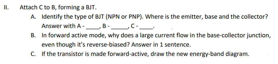
Transcribed Image Text:II.
Attach C to B, forming a BJT.
A. Identify the type of BJT (NPN or PNP). Where is the emitter, base and the collector?
Answer with A -_B -
C-
In forward active mode, why does a large current flow in the base-collector junction,
even though it's reverse-biased? Answer in 1 sentence.
C. If the transistor is made forward-active, draw the new energy-band diagram.
Transcribed Image Text:A
В
E.
EF
E.
E,
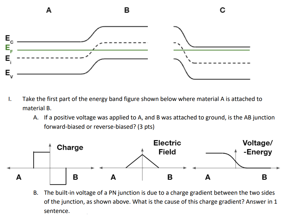
I.
Take the first part of the energy band figure shown below where material A is attached to
material B.
A. If a positive voltage was applied to A, and B was attached to ground, is the AB junction
forward-biased or reverse-biased? (3 pts)
Voltage/
-Energy
Electric
Charge
Field
A
В
A
A
В
B. The built-in voltage of a PN junction is due to a charge gradient between the two sides
of the junction, as shown above. What is the cause of this charge gradient? Answer in 1
sentence.
u°w* w¯ w?
Expert Solution
This question has been solved!
Explore an expertly crafted, step-by-step solution for a thorough understanding of key concepts.

This is a popular solution!

Trending now
This is a popular solution!

Step by step
Solved in 2 steps with 2 images

Knowledge Booster


Learn more about
Need a deep-dive on the concept behind this application? Look no further. Learn more about this topic, electrical-engineering and related others by exploring similar questions and additional content below.Recommended textbooks for you
Introductory Circuit Analysis (13th Edition)
Electrical Engineering
ISBN:
9780133923605
Author:
Robert L. Boylestad
Publisher:
PEARSON

Delmar's Standard Textbook Of Electricity
Electrical Engineering
ISBN:
9781337900348
Author:
Stephen L. Herman
Publisher:
Cengage Learning

Programmable Logic Controllers
Electrical Engineering
ISBN:
9780073373843
Author:
Frank D. Petruzella
Publisher:
McGraw-Hill Education
Introductory Circuit Analysis (13th Edition)
Electrical Engineering
ISBN:
9780133923605
Author:
Robert L. Boylestad
Publisher:
PEARSON
Delmar's Standard Textbook Of Electricity
Electrical Engineering
ISBN:
9781337900348
Author:
Stephen L. Herman
Publisher:
Cengage Learning
Programmable Logic Controllers
Electrical Engineering
ISBN:
9780073373843
Author:
Frank D. Petruzella
Publisher:
McGraw-Hill Education

Fundamentals of Electric Circuits
Electrical Engineering
ISBN:
9780078028229
Author:
Charles K Alexander, Matthew Sadiku
Publisher:
McGraw-Hill Education

Electric Circuits. (11th Edition)
Electrical Engineering
ISBN:
9780134746968
Author:
James W. Nilsson, Susan Riedel
Publisher:
PEARSON

Engineering Electromagnetics
Electrical Engineering
ISBN:
9780078028151
Author:
Hayt, William H. (william Hart), Jr, BUCK, John A.
Publisher:
Mcgraw-hill Education,