Part c) 3. The Qo output of the counter shown a. is present before Qi or Q2 b. changes on every clock pulse c. has a higher frequency than Q1 or Q2 d. all of the above MIGH GL O Choice d O Choice a O Choice c O Choice b
Part c) 3. The Qo output of the counter shown a. is present before Qi or Q2 b. changes on every clock pulse c. has a higher frequency than Q1 or Q2 d. all of the above MIGH GL O Choice d O Choice a O Choice c O Choice b

Chapter22: Sequence Control
Section: Chapter Questions
Problem 6SQ: Draw a symbol for a solid-state logic element AND.

Related questions
Question
100%
PLEASE HELP ON PART A,B,C
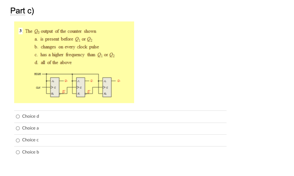
Transcribed Image Text:Part c)
3. The Qo output of the counter shown
a is present before Qi or Q2
b. changes on every clock pulse
c. has a higher frequency than Q1 or Q2
d. all of the above
MIGH
O Choice d
O Choice a
Choice c
O Choice b
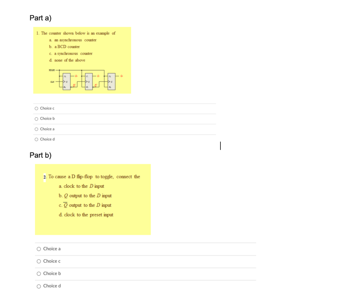
Transcribed Image Text:Part a)
1. The counter shown below is an example of
a. an asynchronous counter
b. a BCD counter
c. a synchronous counter
d none of the above
HIGH +
O Choice c
O Choice b
O Choice a
O Choice d
Part b)
2. To cause a D flip-flop to toggle, connect the
a. clock to the D input
b. Q output to the D input
c. Q output to the D input
d. clock to the preset input
O Choice a
O Choice c
O Choice b
O Choice d
Expert Solution
This question has been solved!
Explore an expertly crafted, step-by-step solution for a thorough understanding of key concepts.

This is a popular solution!

Trending now
This is a popular solution!

Step by step
Solved in 2 steps with 2 images

Knowledge Booster


Learn more about
Need a deep-dive on the concept behind this application? Look no further. Learn more about this topic, electrical-engineering and related others by exploring similar questions and additional content below.Recommended textbooks for you