Please can you explain and show every calcul and details I am confused how to solve this
Please can you explain and show every calcul and details I am confused how to solve this

Power System Analysis and Design (MindTap Course List)
6th Edition
ISBN:9781305632134
Author:J. Duncan Glover, Thomas Overbye, Mulukutla S. Sarma
Publisher:J. Duncan Glover, Thomas Overbye, Mulukutla S. Sarma
Chapter4: Transmission Line Parameters
Section: Chapter Questions
Problem 4.2P: The temperature dependence of resistance is also quantified by the relation R2=R1[ 1+(T2T1) ] where...

Related questions
Question
Please can you explain and show every calcul and details I am confused how to solve this
Transcribed Image Text:+ New
O
su
B
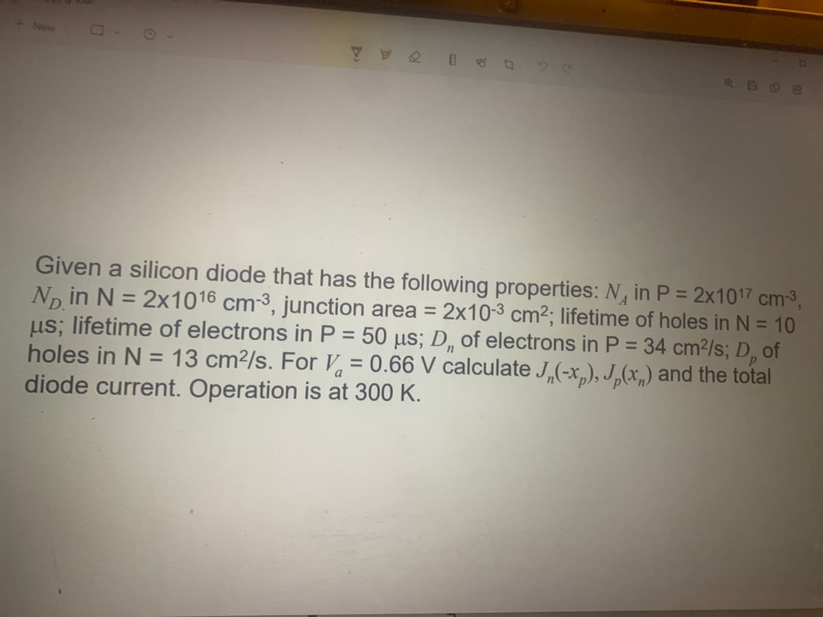
Given a silicon diode that has the following properties: N₁ in P = 2x10¹7 cm-³,
No in N= 2x1016 cm-3, junction area = 2x10-³ cm²; lifetime of holes in N = 10
us; lifetime of electrons in P = 50 µs; D₁ of electrons in P = 34 cm²/s; D, of
holes in N = 13 cm²/s. For V₁ = 0.66 V calculate J(-x), Jp(x) and the total
diode current. Operation is at 300 K.
n
Expert Solution
This question has been solved!
Explore an expertly crafted, step-by-step solution for a thorough understanding of key concepts.

Step by step
Solved in 3 steps with 3 images

Knowledge Booster


Learn more about
Need a deep-dive on the concept behind this application? Look no further. Learn more about this topic, electrical-engineering and related others by exploring similar questions and additional content below.Recommended textbooks for you
Power System Analysis and Design (MindTap Course …
Electrical Engineering
ISBN:
9781305632134
Author:
J. Duncan Glover, Thomas Overbye, Mulukutla S. Sarma
Publisher:
Cengage Learning

Power System Analysis and Design (MindTap Course …
Electrical Engineering
ISBN:
9781305632134
Author:
J. Duncan Glover, Thomas Overbye, Mulukutla S. Sarma
Publisher:
Cengage Learning