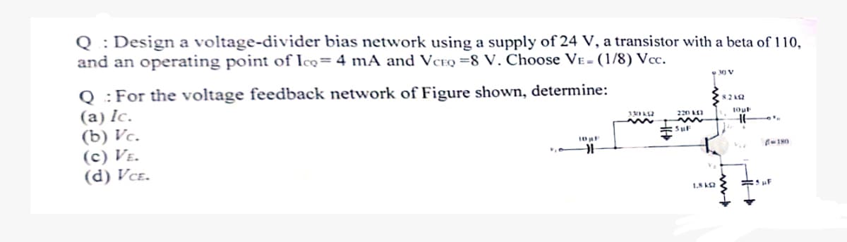
Q: Design a voltage-divider bias network using a supply of 24 V, a transistor with a beta of 110, and an operating point of Ico= 4 mA and VCEQ=8 V. Choose VE- (1/8) Vcc. Q: For the voltage feedback network of Figure shown, determine: 30 V (a) Ic. (b) Vc. (c) VE. (d) VCE. (8.2k 330492 22012 10pF w SuF 1.8 k www-b 16 -180 F


Q: None
A: Step 1: Step 2: Step 3: Step 4:
Q: Calculate the Fourier transform of the following functions using the shift theorem
A: To find the Fourier transform of the given functions using the shift theorem, we need to remember…
Q: I have a 230/460 volt motor, rated 1140 rpm at 60 hz. can you please tell me the number of poles and…
A: The objective of the question is to determine the number of poles in the motor and its rated power…
Q: Question 1: The characteristic table of a sequential logic circuit with inputs (a, b) is given…
A: Solution :The given characteristic table of a sequential logic circuit is:abQ(t+1)000101x1Q(t)(a)…
Q: 5.6 A sequential circuit with two D flip-flops A and B, two inputs, x and y; and one output z is…
A:
Q: Create schematic diagrams showing the working principle of the most widely used renewable energy…
A: I answered this question based on the given topic you provided and did some research to support my…
Q: Sove differential equation using laplace transform: dy(t)/dt + 2y(t) = 3u(t) Initial condition…
A: Sure, I can help you solve the differential equation dy(t)/dt + 2y(t) = 3u(t) using the Laplace…
Q: Show all work please
A: Step 1: Step 2: Step 3: Step 4:
Q: 1. Consider the circuit shown below. The circuit is in steady state prior to /= 0. (a) What is v(0)?…
A: a. Inductors resist changes in current. In the steady state, before the switch is closed at t=0, the…
Q: 4.2. The illumination levels in two different points, 0.75m away from each other, are 450 and 275…
A: Given:The illumination levels in two different points 0.75 m away from each other are 450 and 275…
Q: (b) i(t) (t = 50ms is period of waveform b.) here is my answer i(t) = 10sin(125.66t + 120o)A can you…
A:
Q: Convert the following decimal number to the binary format: 15 (in decimal) = (in binary) O 1011 O…
A:
Q: What symbol is used to identify edge-triggered flip-flops? The letter E on the Enable input A bubble…
A: Question 7 :-Ans:-A triangle on the Clock inputThe symbol used to identify edge-triggered flip-flops…
Q: 7. For the circuit shown below: a) Calculate the real and reactive power associated with each…
A: Step 1: Analysis of circuit Step 2: Part aStep 3: Part b Step 4:Part C
Q: Given this circuit, how can the equivalent resistance be found by terminals a and b if the overall…
A:
Q: None
A:
Q: 9) (a) Consider a linear time-invariant system whose transfer function is H(f) = -0.01|f| + 1.…
A: Question 9 a):Steps to solve:First lets rewrite the transfer function H(f) in terms of s, using the…
Q: what is the current through the 6 ohm resistor? D ง 2 V₂ 492 w V3 V₁ 7V 5Ω ww 2. ? 32 392 4A 4 ли ន…
A:
Q: Two long, parallel conductors, separated by 11.0 cm, carry currents in the same direction. The first…
A: Step 1:Step 2:Step 3: Step 4:
Q: If the feedback resistor in an non-inverting opamp is open, the voltage gain increases decreases is…
A: If the feedback resistor in a non-inverting op-amp configuration is open (i.e., removed), the…
Q: Consider a regulator system with a plant given by: 0 1 0 x = Ax+ Bu, A = 0 0 1 B = 0 L-1 -5 -6] The…
A: To design a state feedback controller for the given system, we need to compute the gain matrix ( K )…
Q: Use servo motor to be rotates to right from 10 to 150 degrees with step of an angle of 10 degrees,…
A: Given:Servo motor to be rotates to right from 10 to 150 degrees with step of an angle of 10 degrees,…
Q: The output voltage of a single-phase full-bridge inverter is controlled by pulse-width modulation…
A: To determine the required pulse width for the fundamental RMS component to be 70% of the DC input…
Q: Please refer to the parallel-basedclipper circuit shown below for this problem.For simplicity,…
A: Step 1: Step 2:
Q: QUESTION 2 Identify which safety equipment was used when you soldered the PCB (choose all which…
A: Typically, the following safety gear is utilised when soldering a PCB:• A. Safety glasses: They…
Q: Design and simulate series and parallel RLC circuits with LTspice to demonstrate different damped…
A: General Explanation:For a simple RLC circuit, the following parameters define the transient behavior…
Q: Question #8 The operational amplifier in the circuit shown in Fig. P18.8 is ideal. Find the &…
A:
Q: The buck regulator in the next figure has an input voltage Vs = 15 V. The required average output…
A: If critical capacitance is needed at nominal inductance value, put L=11.05mH instead of 0.184mH.…
Q: If the equivalent resistance is 4K ohm as seen by the source, show the steps to find this and the…
A:
Q: Create Truth table and logic diagram using basic gates F = X +YZ
A: The objective of the question is to create a truth table and logic diagram for the given Boolean…
Q: Given the following open-loop system G(s) = 20(s+2) s(s+4)(s+6) design a feedback controller u =…
A: (2). Closed-loop system in state-space formulation:-Once we have the state-space representation of…
Q: Q2) A 220-V, 3-op, 4-pole, 50-Hz, Y-connected induction motor is rated 3.73 kW. The equivalent…
A: i) To find the input current of the motor, we need to calculate the total impedance of the motor at…
Q: Q1/Answer the following questions? 1. List and explain LCD registers? 2. Human eyes emit- -energy…
A: The full form of LCD is liquid crystal display and the full form of LED is light emitting diode. Now…
Q: d) Explain how/why Y3 (k) resembles a delta impulse in frequency domain (what does the periodic…
A: Given:To do:d) How/why Y3(k) resembles a delta impulse in frequency domain?e) Sketch Y3(k) points on…
Q: Whenever current in an inductor changes: Select one: the coil inductance changes. induced voltage…
A: The objective of the question is to understand the behavior of an inductor when the current flowing…
Q: Please answer in typing format
A:
Q: Design a circuit that amplifies a 500 mV signal originating from a computer keyboard, so that this…
A: To amplify a 500 mV signal from a computer keyboard for interpretation by digital circuits on a…
Q: A customer has sent in a transformer for repair, with the following information on its nameplate: Dz…
A: Grouping transformers is necessary for several reasons:Voltage Compatibility: Transformers are often…
Q: Answer the following questions with the circuit drawn: a)calculate the sum of currents at node A…
A: KIRCHHOFFS CURRENT LAW: It states that the algebraic sum of currents entering into the node is…
Q: What results when you open the circuit and stop current to an inductor? Select one: counter voltage…
A: The question is asking about the behavior of an inductor when the circuit it is part of is opened,…
Q: This is a practice question from the Signal and Systems course of my Electrical Engineering Program.…
A: Step 1: Step 2: Step 3: Step 4:
Q: 0.752 0.1252 = Q4) Determine the discrete Fourier transform DFT of x(n) (1.2,3,4) Good luck
A:
Q: no ai, answer pkz,fast
A: Approach to solving the question:Calculate the entropy (Part a): Use the formula for entropy to…
Q: 4) This circuit employs negative feedback near-zero frequencies to prevent "latch-up" and has two…
A: In order for a circuit to oscillate, it must meet two conditions known as the Barkhausen criteria.…
Q: The single-phase half-bridge inverter has a resistive load of R 52 and the dc input voltage is Vs =…
A: Step 1: Step 2:
Q: Q: A 3 phase 10 MVA, HI KV Y connected alternator is protected by Merz-Price -circulating current…
A:
Q: Theme fouriertransform: Find the solution to what is in the image that satisfies y(0) = 0 y(t) =
A:
Q: ၁ B ☑ IB Vcc BIB E w Rc C
A: Approach to solving the question: Using the components and transistor terminals you mentioned, you…
Q: Q1: Consider the finite-length sequence 6(n) +28(n-5) x(n) (a) Find the 10-point discrete Fourier…
A: Step 1Step 2Step 3Step 4 :Step 5
Q: I need the expert's solution handwritten.
A: A:Answer:B:C:

Step by step
Solved in 2 steps with 3 images

- Design a Single-Stage Common Emitter Class A Amplifier Specifications:Voltage Divider Bias Circuit Supply: Any value from 10Vdc to 24VdcLoad: 1kΩVoltage Gain: Any value from 80 to 400Lower Cutoff Frequency: 100 HzSinusoidal source (zero internal resistance): 50mVp-pTransistor: Si, β = 75 • Base-Collector capacitance = 8pF • Base-Emitter Capacitance = 25pF a) compute for the biasing resistances.b) determine the dc transistor terminal voltages and transistor currents.Vs=100 mV peak-to-peak, 1 kHz sine signal, Kn=0.4mA/v^2 ,Vt=1V , λ=0.01V^-1 Make the DC analysis of the above given mosfet amplifier circuit. Simulation to tableWrite down the measured values and mathematical calculation results. (The valueswith the units.)DC Parameters ,Measured value ,Calculated ValueVGETCVGSVDVDSIDb. Draw the small signal model for the AC analysis of the circuit. Find the gm, ro, Av values.c. Show the Vs input signal and the Vo output signal of the circuit on the oscilloscope. Volt/div of channels andSpecify time/div values.Instruction/s: Draw, Illustrate and label your schematic diagram before solving the problem.2.) Given a Collector -Feedback Biased transistor circuit with voltage at common collector is +10v ,base resistor is 100k ohms, Collector resistor is 10k ohms and Base current is 8.38 micro ampere, ,Voltage at Base-emitter junction is 0.7v. Determine Beta DC , Collector current and Voltage at collector-emitter junction. These might help as a guide to answer the problem...
- Design a two-stages amplifier circuit MOSFET-BJT (no bypass for the second BJT, all BJTs are in maxswing condition)Rin=1 million Ohm, Rout=4K Ohm, Gv=15. The input signal is a sine signal, amplitude=1 V, F=1K Hz and the resistance=100K OhmIn the circuit given in the figure, Vcc = 15 V, R1 = R2 = 10kΩ, RE = 1KΩ, RL = 0.5kΩ and transistor parameters are given as VBE = 0.7V, ßdc = ß0 = 100. a. Calculate the values of DC bias currents and voltages (IBQ, ICQ and VCEQ). b. Draw the small signal equivalent circuit of the circuit using the hybrid model of the transistor. c. Derive the input impedance expression of the circuit and calculate its value. d. Derive the AVI and AVG voltage gain expressions and calculate their values. e. Derive the current gain expression AI = I0 / Ii and calculate its value. Compare this value you have calculated with the value you will calculate using the expression Aİ = Zi AVI / RL.The given circuit is a 2N4403 PNP common collector amplifier. Let VCC=12V, VEE=-12V, R1=52.5kΩ, R2=33kΩ, and RE=2.5kΩ. Determine IB, IC, IE, VB, VC, and VE. Start by initially assuming |VBE| =0.7V or and assuming a value of beta (β). Where to look for the value of β? (Hint: It’s in the transistor model assigned). Determine the input voltage (may extend from the supply voltage range) where the BJT goes from “cut-off to active” and where it goes from “active to saturation”. Assume VCE=0.3V (edge of saturation), RL=500Ω, and C1, C2→∞.
- Enclosed please find an amplifier circuit designed with a BJT transistor. VCC = 9Volt for the circuit. All capacity values are selected sufficiently large. BJT Transistor B = 100 Vbe(on) = 0.8V, VA=100V, Vt= 26mV Vce (sat) = 0.15Volt. Calculate “Vceq” and “Icq “ values at the operating point of the circuit. In what area does this BJT transistor work in? Draw the small signal equivalent circuit of the circuit. Calculate the AC small signal current earnings of the circuit (Ai = I out / I input). Note: Is the current passes over Rs source resistance and The IO current passes over RL source resistance. Please Calculate Rin input resistance?Amplifier circuit is show below has a single ac input and one ac output. Assuming 2N2222 transistor: 1- Determine the Q point, then illustrate it on the transistor I-V characteristic curves. 2- Is the transistor in the active region? Explain thoroughly. 3- Construct the T-model of the transistor with all parameters labelled and evaluated. Assume room temperature. 4- Draw a complete small signal circuit model, then find the voltage gain. Explain two characteristics of this amplifier. 5- Calculate the current gain, the input resistance, and the output resistance.In the common-emitter amplifier circuit shown in the figure, Vcc=9V, R1=27kΩ, R2=15kΩ, RE=1.2kΩ and RC=2.2kΩ. The transistor has β=100.a-) If Rsig=10kΩ and RL=2kΩ, calculate the IE value of the amplifier.b-) For small signal analysis of the transistor, find the value of Rin by deriving the π-modelc-) Calculate vo/vsig and io/ii.
- Design a DC bias circuit for an voltage divider amplifier circuit . Proved design for VCEQ = 8v,Vcc= 20v, β=80 and ICQ=10 mA? VBE =0.7 vCoonsider the common emitter amplifier shown in figure below. Assume a β of 100, VBE = 0.7V, VT = 25mA and VA = 100V. Draw an equivalent DC model and determine the rπ, transconductance (gm) and ro. Draw an equaivalent AC model using the small-signal model Find an expression for vbe and vo in terms of the input voltage2- Draw a transistor amplifier circuit ( BJT ) Bipolar Junction of type ( NPN ) then write the mathematical relation of Circuit voltage gain factor and what is the factors that depend on and how can we increase the gain factor .