Q: For the amplifier characteristics shown in the Figure: 1-Determin Vcc, VCE(cutoff), ltsat), RB,RcB for the fixed- bias configuration shown in Figure b.
Q: For the amplifier characteristics shown in the Figure: 1-Determin Vcc, VCE(cutoff), ltsat), RB,RcB for the fixed- bias configuration shown in Figure b.

Power System Analysis and Design (MindTap Course List)
6th Edition
ISBN:9781305632134
Author:J. Duncan Glover, Thomas Overbye, Mulukutla S. Sarma
Publisher:J. Duncan Glover, Thomas Overbye, Mulukutla S. Sarma
Chapter12: Power System Controls
Section: Chapter Questions
Problem 12.3P

Related questions

Question
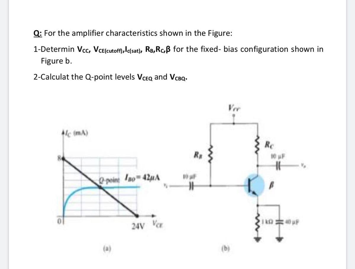
Transcribed Image Text:Q: For the amplifier characteristics shown in the Figure:
1-Determin Vcc, VCE(cutoff), l(sat), RB,Rc,B for the fixed- bias configuration shown in
Figure b.
2-Calculat the Q-point levels VCEQ and VCBQ.
Ver
4c imA)
Rc
10 uF
10 uF
point Iso 42A
24V Ver
Expert Solution
This question has been solved!
Explore an expertly crafted, step-by-step solution for a thorough understanding of key concepts.

Step by step
Solved in 2 steps with 4 images

Knowledge Booster


Learn more about
Need a deep-dive on the concept behind this application? Look no further. Learn more about this topic, electrical-engineering and related others by exploring similar questions and additional content below.Recommended textbooks for you
Power System Analysis and Design (MindTap Course …
Electrical Engineering
ISBN:
9781305632134
Author:
J. Duncan Glover, Thomas Overbye, Mulukutla S. Sarma
Publisher:
Cengage Learning
Power System Analysis and Design (MindTap Course …
Electrical Engineering
ISBN:
9781305632134
Author:
J. Duncan Glover, Thomas Overbye, Mulukutla S. Sarma
Publisher:
Cengage Learning