Q1: For the circuit on the right, a. Graph the output voltage v0 against the input voltage v1. Assume ideal diodes. b. Describe the behaviour of D1 in terms of semiconductor behaviour.


3
Q1:
For the circuit on the right,
a. Graph the output voltage v0 against the input voltage v1.
Assume ideal diodes.
b. Describe the behaviour of D1 in terms of
semiconductor behaviour.
Q2: For the circuit shown in Figure 1:
1. Describe the behaviour of a p-n junction in terms of semiconductor behaviour.
2. Describe and evaluate the circuit. Assume the values for the parameters in the circuit.
You should critically evaluate the performance of the circuit and suggest potential applications.
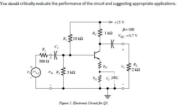
Q3: For the circuit shown in Figure 2, find the following:
1. Describe the function of the circuit in terms of simple of semiconductor behavior.
2. Evaluate the output voltage vo, assuming vs is 10 Sine (200t) mV, RE1 =100 Ω,
and RE2 =900 Ω. The bypass capacitor (CE) is in parallel with RE2.
3. Simulate the circuit and verify your answers; you should show the input voltage.
and output voltage on the same graph.
4. You should explain the characteristics of the amplifier.


Trending now
This is a popular solution!

Step by step
Solved in 2 steps with 1 images


