Q3) For the two stages circuit as shown, find: VIN VOUT CE amplifier CE amplifier HE Z,- 1 k2 Z,= 1 k2 Z, - 3 k2 Z, - 3 kQ R 2 k2 AVN --400 AVN --400 The voltage gain of first stage is equal? The voltage gain of second stage is equal? The total voltage gain in dB is equal?
Q3) For the two stages circuit as shown, find: VIN VOUT CE amplifier CE amplifier HE Z,- 1 k2 Z,= 1 k2 Z, - 3 k2 Z, - 3 kQ R 2 k2 AVN --400 AVN --400 The voltage gain of first stage is equal? The voltage gain of second stage is equal? The total voltage gain in dB is equal?

Power System Analysis and Design (MindTap Course List)
6th Edition
ISBN:9781305632134
Author:J. Duncan Glover, Thomas Overbye, Mulukutla S. Sarma
Publisher:J. Duncan Glover, Thomas Overbye, Mulukutla S. Sarma
Chapter12: Power System Controls
Section: Chapter Questions
Problem 12.3P

Related questions
Question
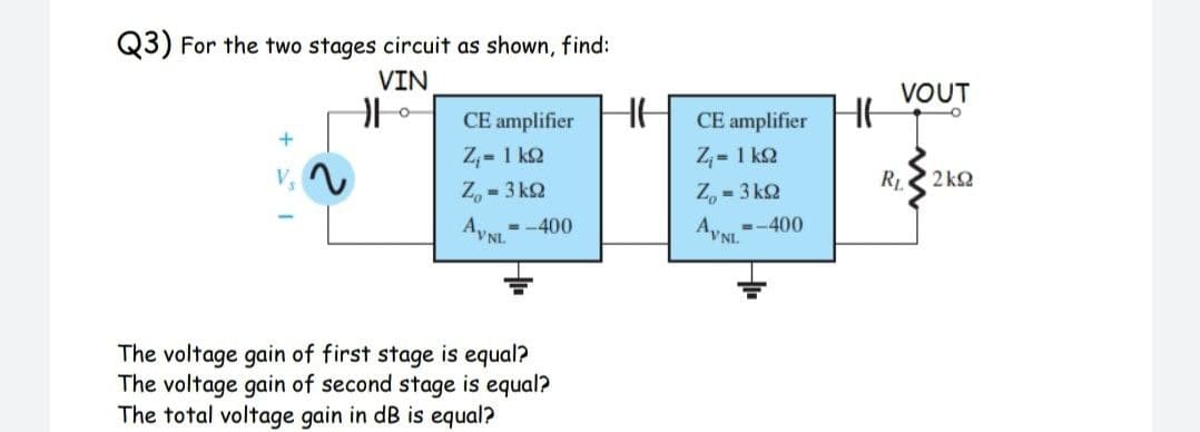
Transcribed Image Text:Q3) For the two stages circuit as shown, find:
VIN
VOUT
HE
CE amplifier
CE amplifier
Z,= 1 k2
Z,- 1 k2
R
2 k2
Z, - 3 kQ
Z, - 3 k2
- -400
Ayst
AVNI =-400
The voltage gain of first stage is equal?
The voltage gain of second stage is equal?
The total voltage gain in dB is equal?
Expert Solution
This question has been solved!
Explore an expertly crafted, step-by-step solution for a thorough understanding of key concepts.

This is a popular solution!

Trending now
This is a popular solution!

Step by step
Solved in 2 steps with 1 images

Knowledge Booster


Learn more about
Need a deep-dive on the concept behind this application? Look no further. Learn more about this topic, electrical-engineering and related others by exploring similar questions and additional content below.Recommended textbooks for you
Power System Analysis and Design (MindTap Course …
Electrical Engineering
ISBN:
9781305632134
Author:
J. Duncan Glover, Thomas Overbye, Mulukutla S. Sarma
Publisher:
Cengage Learning
Power System Analysis and Design (MindTap Course …
Electrical Engineering
ISBN:
9781305632134
Author:
J. Duncan Glover, Thomas Overbye, Mulukutla S. Sarma
Publisher:
Cengage Learning