Task #1: Describe a 4-bit adder. The output of the adder is displayed on two 7-segment displays (Why?). You will make use of the BCH (Binary-Coded Hexadecimal) converter to display the output (i.e. through module instantiation). What should be the bit width of the output signal SUM? D1 Adder SUM D2 1. Create a new Quartus II project. Write a Verilog module that describes the 4-bit adder circuits shown above. Make use of the BCH converter module through module instantiation.
Task #1: Describe a 4-bit adder. The output of the adder is displayed on two 7-segment displays (Why?). You will make use of the BCH (Binary-Coded Hexadecimal) converter to display the output (i.e. through module instantiation). What should be the bit width of the output signal SUM? D1 Adder SUM D2 1. Create a new Quartus II project. Write a Verilog module that describes the 4-bit adder circuits shown above. Make use of the BCH converter module through module instantiation.

Computer Networking: A Top-Down Approach (7th Edition)
7th Edition
ISBN:9780133594140
Author:James Kurose, Keith Ross
Publisher:James Kurose, Keith Ross
Chapter1: Computer Networks And The Internet
Section: Chapter Questions
Problem R1RQ: What is the difference between a host and an end system? List several different types of end...

Related questions
Question
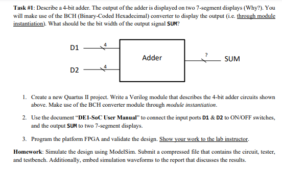
Transcribed Image Text:Task #1: Describe a 4-bit adder. The output of the adder is displayed on two 7-segment displays (Why?). You
will make use of the BCH (Binary-Coded Hexadecimal) converter to display the output (i.e. through module
instantiation). What should be the bit width of the output signal SUM?
D1
Adder
SUM
D2
1. Create a new Quartus II project. Write a Verilog module that describes the 4-bit adder circuits shown
above. Make use of the BCH converter module through module instantiation.
2. Use the document “DE1-SoC User Manual" to connect the input ports D1 & D2 to ON/OFF switches,
and the output SUM to two 7-segment displays.
3. Program the platform FPGA and validate the design. Show your work to the lab instructor.
Homework: Simulate the design using ModelSim. Submit a compressed file that contains the circuit, tester,
and testbench. Additionally, embed simulation waveforms to the report that discusses the results.
Expert Solution
This question has been solved!
Explore an expertly crafted, step-by-step solution for a thorough understanding of key concepts.

This is a popular solution!

Trending now
This is a popular solution!

Step by step
Solved in 2 steps

Recommended textbooks for you
Computer Networking: A Top-Down Approach (7th Edi…
Computer Engineering
ISBN:
9780133594140
Author:
James Kurose, Keith Ross
Publisher:
PEARSON

Computer Organization and Design MIPS Edition, Fi…
Computer Engineering
ISBN:
9780124077263
Author:
David A. Patterson, John L. Hennessy
Publisher:
Elsevier Science

Network+ Guide to Networks (MindTap Course List)
Computer Engineering
ISBN:
9781337569330
Author:
Jill West, Tamara Dean, Jean Andrews
Publisher:
Cengage Learning
Computer Networking: A Top-Down Approach (7th Edi…
Computer Engineering
ISBN:
9780133594140
Author:
James Kurose, Keith Ross
Publisher:
PEARSON
Computer Organization and Design MIPS Edition, Fi…
Computer Engineering
ISBN:
9780124077263
Author:
David A. Patterson, John L. Hennessy
Publisher:
Elsevier Science
Network+ Guide to Networks (MindTap Course List)
Computer Engineering
ISBN:
9781337569330
Author:
Jill West, Tamara Dean, Jean Andrews
Publisher:
Cengage Learning

Concepts of Database Management
Computer Engineering
ISBN:
9781337093422
Author:
Joy L. Starks, Philip J. Pratt, Mary Z. Last
Publisher:
Cengage Learning

Prelude to Programming
Computer Engineering
ISBN:
9780133750423
Author:
VENIT, Stewart
Publisher:
Pearson Education

Sc Business Data Communications and Networking, T…
Computer Engineering
ISBN:
9781119368830
Author:
FITZGERALD
Publisher:
WILEY