The cross section of a simple substrate n-channel MOSFET biased above threshold is illustrated below. VGS > VT VSB=0 VDS=0 n+ p-type substrate What is meant by "pinch-off" in a MOSFET and what happens to the channel when pinch-off occurs? How do we add the effect of channel shortening to the MOSFET square law model when VDs > VDSsat? A gate bias of VGS = 2.5 V is applied to a MOSFET with a threshold voltage of V₁ = 0.4 V and substrate doping of N₁ = 5 x 10¹ cm³. The gate oxide thickness is fox = 20 nm and the device has an effective channel length of 2 µm and width of 10 um. If channel shortening can be ignored, what is the channel current. In. for Vps = 1.5V ? ID=0
The cross section of a simple substrate n-channel MOSFET biased above threshold is illustrated below. VGS > VT VSB=0 VDS=0 n+ p-type substrate What is meant by "pinch-off" in a MOSFET and what happens to the channel when pinch-off occurs? How do we add the effect of channel shortening to the MOSFET square law model when VDs > VDSsat? A gate bias of VGS = 2.5 V is applied to a MOSFET with a threshold voltage of V₁ = 0.4 V and substrate doping of N₁ = 5 x 10¹ cm³. The gate oxide thickness is fox = 20 nm and the device has an effective channel length of 2 µm and width of 10 um. If channel shortening can be ignored, what is the channel current. In. for Vps = 1.5V ? ID=0

Introductory Circuit Analysis (13th Edition)
13th Edition
ISBN:9780133923605
Author:Robert L. Boylestad
Publisher:Robert L. Boylestad
Chapter1: Introduction
Section: Chapter Questions
Problem 1P: Visit your local library (at school or home) and describe the extent to which it provides literature...

Related questions
Question
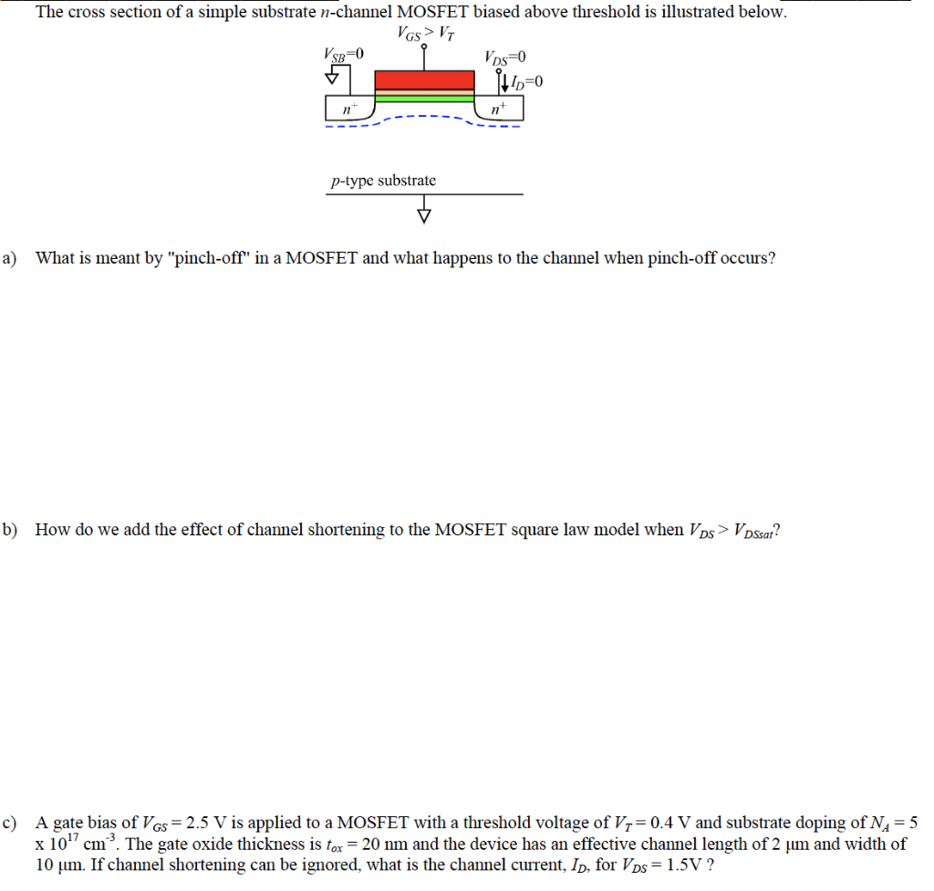
Transcribed Image Text:The cross section of a simple substrate n-channel MOSFET biased above threshold is illustrated below.
VGS > VT
VSB=0
✓
VDS=0
ID=0
n
n+
p-type substrate
a) What is meant by "pinch-off" in a MOSFET and what happens to the channel when pinch-off occurs?
b) How do we add the effect of channel shortening to the MOSFET square law model when VDS> VDSsat?
c) A gate bias of VGS = 2.5 V is applied to a MOSFET with a threshold voltage of VT=0.4 V and substrate doping of N₁ = 5
x 10¹ cm³. The gate oxide thickness is fox = 20 nm and the device has an effective channel length of 2 μm and width of
10 μm. If channel shortening can be ignored, what is the channel current, ID, for VDs = 1.5V ?
Expert Solution
This question has been solved!
Explore an expertly crafted, step-by-step solution for a thorough understanding of key concepts.

Step by step
Solved in 2 steps with 3 images

Knowledge Booster


Learn more about
Need a deep-dive on the concept behind this application? Look no further. Learn more about this topic, electrical-engineering and related others by exploring similar questions and additional content below.Recommended textbooks for you
Introductory Circuit Analysis (13th Edition)
Electrical Engineering
ISBN:
9780133923605
Author:
Robert L. Boylestad
Publisher:
PEARSON

Delmar's Standard Textbook Of Electricity
Electrical Engineering
ISBN:
9781337900348
Author:
Stephen L. Herman
Publisher:
Cengage Learning

Programmable Logic Controllers
Electrical Engineering
ISBN:
9780073373843
Author:
Frank D. Petruzella
Publisher:
McGraw-Hill Education
Introductory Circuit Analysis (13th Edition)
Electrical Engineering
ISBN:
9780133923605
Author:
Robert L. Boylestad
Publisher:
PEARSON
Delmar's Standard Textbook Of Electricity
Electrical Engineering
ISBN:
9781337900348
Author:
Stephen L. Herman
Publisher:
Cengage Learning
Programmable Logic Controllers
Electrical Engineering
ISBN:
9780073373843
Author:
Frank D. Petruzella
Publisher:
McGraw-Hill Education

Fundamentals of Electric Circuits
Electrical Engineering
ISBN:
9780078028229
Author:
Charles K Alexander, Matthew Sadiku
Publisher:
McGraw-Hill Education

Electric Circuits. (11th Edition)
Electrical Engineering
ISBN:
9780134746968
Author:
James W. Nilsson, Susan Riedel
Publisher:
PEARSON

Engineering Electromagnetics
Electrical Engineering
ISBN:
9780078028151
Author:
Hayt, William H. (william Hart), Jr, BUCK, John A.
Publisher:
Mcgraw-hill Education,