The diode emitter resistance, re and draw re transistor model (AC equivalent circuu). The input impedance, Z¡ as seen from the input voltage.
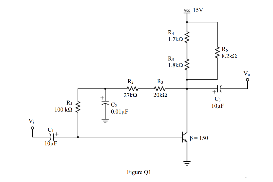
Q: Name: (11) The supply voltage VCC equals 9V. The base resistor Rais 42. Take 0.6V for the knee…
A: For the given NPN transistor circuit we need to calculate collector resistance, collector current…
Q: The on-state conduction losses is low in MOSFET. Select one: O True O False
A: MOSFET is unipolar device is that current is flowing due to majority charge carrier only so there is…
Q: a) Draw the circuit of a common emitter amplifier.
A: The circuit of a common emitter amplifier is given as: where T1 and T2 are the thyristor and D1 and…
Q: n a common collector configuration transistor , the dc current gain is given by * O B+1 O a+1
A: The common collector configuration is shown below:
Q: Solve this: Transistor AC Analysis a. Determine the re b. Calculate the Vb and Vc c. Determine…
A: The required parameters can be calculated by using the DC and AC analysis of the amplifier circuit.
Q: Design a Common Emitter Amplifier with Voltage Divider Bias for the following parameters: VcC = 24V…
A:
Q: 6. Measure the DC voltages VB, VE, and VC using digital multi-meters. Determine the quiescent point…
A:
Q: iii) Explain the operating principle of a single-slope ADC circuit, in your own words
A: The ADC is an analog to digital convertor. The machines understand the digital binary bits in their…
Q: Assume Icq = 3mA, Vceq = 10V for the given transistor circuit. Find the R1 and Rc values. 22V Rc…
A: consider the given question;
Q: 1 The AC input to a common emitter amplifier (Figure 1) is such that it is comparable to thermal…
A:
Q: Example 1: Determine the Quiescent point (Q-point) for the common-emitter circut in figure below and…
A:
Q: For the transistor, because the current in the base terminal controls the current in the collector…
A: To give whether the statement is true or false
Q: EXPERIMENT TO DETERMINE THE OPERATING POINT PARAMETERS, THE FREQUENCY RESPONSE OF COMMON EMITTER…
A: Given data :
Q: Using Flash ADC method to convert the analoge voltage signal to digital (3-bit) ,where Vi=5V and…
A:
Q: Problem No. 1 (PI) For the common-base configuration (re model), an ac signal of 10 mV is applied,…
A:
Q: DISCUSSION: 1- What is transistor? 2- What is the range of a? 3- Why is a is less than unity? 4- Can…
A:
Q: b. For the emitter-bias network in the figure to the left, determine: Івo and lco. VCEQ VC, VB. VE…
A:
Q: Consider the circuit given below, where R- 1.5 kQ. Both the transistors have a dc and ac current…
A: Given, R1=1.5kΩβDC=βAC=150 where,Vth=Vcc×R2R1+R2=15×11+1.5=6.52 VRth=R1×R2R1+R2=0.565kΩ
Q: ------ the emitter voltage For pnp transistor in the active mode, the base voltage is O greater than…
A: Answer: less than Explanation: a. It is not a valid option. if the base voltage is greater than…
Q: region. For the transistor in the shown figure, it operates in Vce +8 V Rc 390 2
A:
Q: Design a regulator circuit as given below for V = 16V and V, = 12V. The powers dissapated by the BJT…
A:
Q: Which topology provides the smallest output terminal impedance? O A. Common Emitter O B. Common Base…
A: Consider that in case of the common collector amplifier configuration the impedance is higher on the…
Q: Problem No. 1 (PI) For the common-base configuration (re model), an ac signal of 10 mV is applied,…
A: In this question we will find output voltage in common base configuration..
Q: In the voltage divider bias find the value of emitter voltage and emitter to collector voltage if we…
A:
Q: Attached please find plot of my question regarding Mosfet Transistor. For a Enhancement type…
A: DC analysis of the amplifier will be
Q: For the circuit Shown infiyure Vec %3D RB ERC RB-330k&,ß=80 Find 1 9) 2. 斤hdz Note: When the out Put…
A: Considering the dc biasing and ignoring the ac signal. Applying KVL(Kirchhoff's Voltage Law) from…
Q: A common emitter class A transistor power amplifier uses a transistor with B=100. The load has a…
A:
Q: A MOSFET has . . terminals Select one: a. five O b. two c. three
A: The MOSFET has
Q: 2. From physical analysis why Is is far smaller than lc ? 3. How must the two transistor iunctions…
A: in this question, we have to find out the reason why base current is smaller than collector…
Q: The ac output equivalent circuit of a transistor is as shown in the figure. It is known that this…
A:
Q: What are important aspects of using a MOSFET? O Great efficiency O Can operate at low voltages O…
A: About MOSFET
Q: 4. This symbol is for 5. If a three stage amplifier has individual stage gains of 10db, 6db and…
A: The symbol given is Thyristor If a three stage amplifier has individual gain = 10 db,6 db and 15…
Q: Draw the circuit diagram of a resistance–capacitance coupled source follower
A: A resistance capacitance coupled source follower know as RC coupling is most widely used technique…
Q: In an n-p–n transistor in the common emitter configuration, an ac input signal of ± 50 mV is…
A: Given, AC input, Vin=±50 mV βdc=90, βac=120 VB= 0.7V, IB=17mA, Ib=±7 mA
Q: Draw an I/V characteristic diagram to connect the common emitter, indicating on it the operating…
A: Given:- Common Emitter Configuration:
Q: 1. Given the circuit D, RV a. Derive Kerit and Reritas a function of duty cycle and switching time,…
A: Note: We are authorized to answer three subparts at a time since you have not mentioned which part…
Q: Quèstion 9 In D-MOSFET, Ipss is the maximum Drain current True False
A: Given IDSS in MOSFET is the maximum drain current.
Q: Vo Vs (E Rz Re The following parameter for this transistor, VCC = 5V, RL = 4k2, RE = 3kN, R1 = 60k2,…
A:
Q: Electrical Engineering A uniformly doped silicon pnp bipolar transistor is to be designed with NĘ =…
A: This Question is from Electronics Devices and circuit.
Q: ID a) For a D-MOSFET , prove that : Vs=VGSoff (1– v- IDSS' | b) For a E-MOSFET, prove that : gm=2VK…
A: (II) (a) It is given that: For a D-MOSFET: To prove: VGS=VGSoff1-IDIDSS
Q: List the elements included in the total input resistance of a common-collector amplifier. What is…
A: Given: List the elements included in the total input resistance of a common-collector amplifier and…
Q: 5- For the differential amplifier given in Figure below, the dc emitter current IE is (a) 2.5 mA (b)…
A:
Q: The dc load line on a family of collector characteristic curves of a transistor shows the active…
A: we need to identify what the DC load line on a family of collector characteristic curves of a…
Q: The maximum junction temperature of a transistor is 150°C and the ambient temperature is 25°C. If…
A: Given: The maximum junction temperature of a transistor is 150°C The ambient temperature is 25°C…
Q: A collector modulator is a balanced modulator. O True False The information or intelligence is at…
A: Given Few true or false questions based on modulation. Please find the below attachment for clear…
Q: analysis of transistor biasing circuits, coupling capacitors should be open circuit. In ac True…
A: Choose the correct option In ac analysis of the BJT, coupling capacitor act as open circuit " Is it…
Q: An npn transistor circuit as shown in figure below has a = 0.985 and VBE= 0.3V. If Vcc=16V,…
A:
Q: Quèstion 18 In D-MOSFET, Ipss is the maximum Drain current True False
A:
Q: Il-(a) State the fundamental operating principle of the field-effect transistor as a switch. (b)…
A: Transistor- Transistor is a device which regulates flow of current and also works as switch.
Step by step
Solved in 4 steps with 4 images
- What is CEMF?(i) With neat sketch explain the cross sectional view and I-V characteristics of the device which is used in low on state loss and small switching frequency operations. (ii) Write FOUR demerits of the above mentioned power semiconductor device.The dc load line on a family of collector characteristic curves of transistor shows the........ Choose correct answer : A) All operating regions B) cut-off region only C) active region only D) saturation region only
- For an NPN Bipolar Junction Transistor base-emitter voltage, VBE is 0.7 V at collector current,Ic of 1mA. Calculate the saturation current, emitter-base voltage, emitter current whencollector current is (X+2) mA. Assume β =100 and T=300 K for your calculation.Explain why there is phase inversion in common emitter amplifier.Solve this: Transistor AC Analysis a. Determine the re b. Calculate the Vb and Vc c. Determine the Zi, Zout, and Av
- Subject:Electronics Engineering With a neat circuit diagram, explain the Voltage Divider Bias circuit using approximate analysis. Also derive the equation of stability (S) for Voltage Divider Bias circuit.Describe the basic principle of operation of a bipolar junction transistor. Includeexplanation for the following:i. When minority carriers flow across the transistorii. why the collector current is almost unaffected by the collector potentialA Bipolar junction Transistor with curreat amplification factor being 100, Input Base current is 50μA. Collector voltage is 10 V and biasing voltage being +20 V. Find followings a. Collector current b. Resistance (R1) c. Collector voltage , Emitter voltage , Base Voltage & Collector-Emitter Voltage.