VDD=10V 2. Consider the MOSFET amplifier in Figure 2 with the parameters Kn = 1 mA/V2 and VTN = 2 V. Determine the resistor values to obtain roughly Ip = 1 mA and to set VD approximately midway between VDp and Vg. RD io R1 oVD VG R2 Rs Vss=-10V Figure 2
VDD=10V 2. Consider the MOSFET amplifier in Figure 2 with the parameters Kn = 1 mA/V2 and VTN = 2 V. Determine the resistor values to obtain roughly Ip = 1 mA and to set VD approximately midway between VDp and Vg. RD io R1 oVD VG R2 Rs Vss=-10V Figure 2

Chapter25: Television, Telephone, And Low-voltage Signal Systems
Section25.1: Television Circuit
Problem 5R: From a cost standpoint, which system is more economical to install: a master amplifier distribution...

Related questions

Question
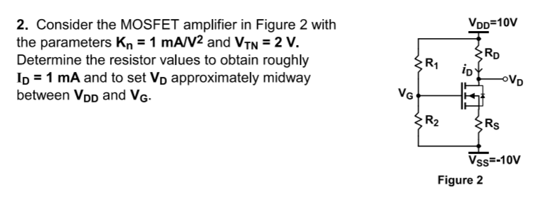
Transcribed Image Text:VDD=10V
2. Consider the MOSFET amplifier in Figure 2 with
the parameters Kn = 1 mA/V² and VTN = 2 V.
Determine the resistor values to obtain roughly
Ip = 1 mA and to set Vp approximately midway
between VDD and VG-
RD
io
R1
oVD
VG
R2
Rs
Vss=-10V
Figure 2
Expert Solution
This question has been solved!
Explore an expertly crafted, step-by-step solution for a thorough understanding of key concepts.

This is a popular solution!

Trending now
This is a popular solution!

Step by step
Solved in 4 steps with 8 images

Knowledge Booster


Learn more about
Need a deep-dive on the concept behind this application? Look no further. Learn more about this topic, electrical-engineering and related others by exploring similar questions and additional content below.Recommended textbooks for you
EBK ELECTRICAL WIRING RESIDENTIAL
Electrical Engineering
ISBN:
9781337516549
Author:
Simmons
Publisher:
CENGAGE LEARNING - CONSIGNMENT
EBK ELECTRICAL WIRING RESIDENTIAL
Electrical Engineering
ISBN:
9781337516549
Author:
Simmons
Publisher:
CENGAGE LEARNING - CONSIGNMENT