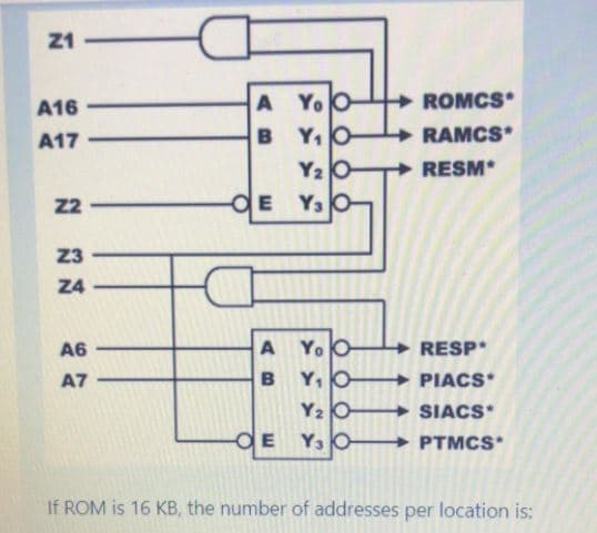
Z1 ROMCS A YoO B YO Y2 O A16 A17 + RAMCS RESM* 22 dE YO Z3 Z4 A6 A Yo O RESP B YO- Y2 O OE Y O A7 PIACS SIACS PTMCS If ROM is 16 KB, the number of addresses per location is:


Q: Question 4 a) Convert the following decimal numbers to their binary equivalents I. 64 II. 128 III.…
A:
Q: Q12/Assume that the microprocessor can directly address 1M with a and 8 data pins, The maximum RAM…
A: We need to find out total capacity for RAM capacity .
Q: The lowest address contained in the ROM memory is: A13- A12- All C B 1 A10- El A 2 ROM 7 CS 0000…
A: The explanation is as follows.
Q: A Karnaugh map is a of the logic system. O a. none of the above O b. Logical representation O c.…
A: A karnaugh map is a -------of the logic system. a.none of the above b.logical representation c.data…
Q: 3. A 50 W TV can operate using a100 W inverter without any problems. a. Yes b. No c. Nor Yes or No
A: Solution-Yes 50 watt tv operate using 100watt inverter
Q: Implement the following functions using a single 8 x 4 ROM. Use dot notation to indicate the ROM…
A: W = A'B + B'C + AC' => W = A'B(C+ C') + B'C(A + A') + AC'(B + B') => W = A'BC + A'BC' + AB'C +…
Q: 3. Implement the following functions using a single 8 × 4 ROM. Use dot notation to indicate the ROM…
A: Write the given function expressions as below and write it in standard form.…
Q: Q12/Assume that the microprocessor can directly address 1M with a and 8 data pins, The maximum RAM…
A: We need to find out maximum ram can be disign by using given chips .
Q: b. Comment with your own words the below instructions. The instruction Comment of the instruction…
A: The instruction always @(XW) reg[2:0]y,Y; if(y==s3 | y==s4)z=1; s2: if(w) Y=s0; else Y=s3;
Q: (3, Discuss the forinciple of coosking - phase bridge inverter dingram woork a three affropriale…
A:
Q: Assume that the microprocessor can directly address 1M with a and 8 data pins. The maximum RAM…
A: Consider that the microprocessor can directly address 1M with a and 8 data pins. The maximum RAM…
Q: Q4. By using Karnaugh map, reduce the combinational logic circuit in Figure 1 to a minimum form. А в…
A: By using karnaugh map method, reduce the following given logic circuit diagram to a minimum form.…
Q: Calculate power absorbed by 20 Ω load in 3-∅ 120° Voltage Source Inverter if the value of DC supply…
A:
Q: Computer M has 8-bit memory width with 8-bit address as illustrated in Figure Memory Memory Address…
A: An Big-endian or a little-endian are the two methods of storing data in the memory locations. In the…
Q: dout din ROM A0-A9 1KX8 cs By using above ROM and 3:8 decoder design memory of size 8KX8
A: Decoder circuit have more output than input. Decoder is combinational circuit that convert n bit…
Q: Question 12 For foxs)-xy-2 yz, implemeat a circuit using one 2-to-1 MUX, two logic gates, the z…
A: We have to find the correct option
Q: 2) Draw the logic circuit A) Y= (A+B+C)DE Y =ABCDE B) X= ACD+BC
A:
Q: Consider the n-input logic gate shown below that operate with the following voltage thresholds: Vol…
A: A logic gate is a model of a digital electronic device, it can any number of inputs but can have…
Q: ii) For the circuit shown in Figure B9, a. Find logic functions for Y and Z. b. Simplify function Z…
A: Solution: Here in this question first of all we simplified the given logic diagram. Here we…
Q: A full adder function is given in Figure 2(a). Implement this function using decoder 74x138 given in…
A: In a combinational circuit, the output only depends on the value of input as regards the previous…
Q: 1) Write simple instructions (simple program) that will add two consecutive bytes of data storied…
A: KEY POINTS OF MICROPROCESSORS 8085 It is manufactured NMOS technology. It is upward compatible with…
Q: $x (2?)dz ,is 5. the system y (t) = a) memoryless, invertible c) memoryless, non-invertible b)…
A:
Q: What is it: Microprocessor/Cache Memory/SRAM/DRAM/EPROM Vce - Vss 23 D3 22 D2 How many addressable…
A: Soluiton a) Since it has 24 pins ,This structure is called 16mb (4MBx4)It has memory package and…
Q: (a) Describe TWO (2) advantages of DIGITAL over to ANALOG in data storage. (1 mark) (b) As…
A: (A): Advantages of digital over analog signals: Digital signals are less affected by the effects of…
Q: 4. Show how to connect two of the 6264C RAM chips symbolized in the figure below to produce a 16K X…
A: Given: The 6264C RAM chips symbolized in the figure below to produce a 16K X 8 RAM module. The…
Q: 3. Implement the following functions using a single 8 × 4 ROM. Use dot notation to indicate the ROM…
A: A ROM is a permanent memory. Its internal structure comprises two basic components: decoder and OR…
Q: Q2 : For the following logic circuits, draw the ladder diagram equivalents: XL YO SO X2 X2 X1 Y1 S1…
A: The given circuit diagrams are:
Q: 1 Simplify the following logical expression and implement them using suitable logie gates. a. F =…
A:
Q: Q13/Assume that the microprocessor can directly address 64K with a and 8 data pins The memory map…
A: We need to select address for chips .
Q: RAM 이 256 X 4 A. The number 5 is being written to the memory at address location 203. B. The chip…
A: option A is not correct because the Address location is 211H not 203H. Option B is not correct…
Q: Q3=100011 solve Q3 O Q3=010110 Q3=110011 Q3/Assume that the microprocessor can directly address 64K…
A: We need 4 memory of 8k * 8 for 16k * 16 , We need to find out address for 4 memory .
Q: Construct a 4-bit parallel adder using gates and fill in the table below. Binary Input Binary Input…
A: The parallel adder circuit is made from a full adder circuit. Four full adders are connected in…
Q: b) The diode is to be used in the AND logic circuit shown in figure Q1b : VDD R VA VB 0 0 0 1 Vo…
A: Given: The diode is to be used in the AND logic circuit shown in the figure below: The inputs are…
Q: Täšk 3: Writé ăñ assemblyprogram that con function. Your program can assume the input has already…
A: he identified variable is only X. DATA SEGMENT X DB 8 ENDS CODE SEGMENT ASSUME DS: DATA CS: CODE…
Q: In the given circuit, 7483 are additions and 7485 comparisons. Four-bit X and Y numbers are applied…
A: IC 7483 is a 4-bit adder IC and IC 7485 is a 4-bit magnitude comparator.
Q: The capacity of a memory of is 14 KB, which is divided into two parts:cells with the addresses from…
A: 1) Registers ar a form of memory used to quickly settle for, store, and transfer knowledge and…
Q: Given a 2 input-4 column 3-output programmable logic array (PLA) device as shown in Figure Q2(e).…
A:
Q: Assume that the microprocessor can directly address 64K with a R/W' and 8 data pins The memory map…
A: Given: The microprocessor can directly address 64K with an R/W' and 8 data pins. To find: The memory…
Q: Chapter #1 Programmable Logic Devices HW # 03 Q. Show how the PAL-type array in Figure below should…
A:
Q: How can I create a circuit based on the table below, I have 2 inputs and 2 outputs. I would like to…
A:
Q: Explain the process of the following Load D3 · D3 12 12 D2 Do Clock D Load Block Diogram of 4-bit…
A: Given
Q: Exercise#1: The following circuit is used as a logic circuit fined the relationship between the…
A:
Q: Negative AND Gate is IC 7432 IC 7408 IC 7402 IC 7400 In static RAM, the memory refreshing circuit is…
A: We need to select correct option.
Q: 1) Write simple instructions (simple program) that will add two consecutive bytes of data storied…
A: Here the given questions has the multiple sub-parts.we will answer few questions for you.If you want…
Q: - is used to exchange the content of memory * location [3000]. [3001] with DX register The…
A: DX register: It is a general-purpose data register. It has 16 bits which are divided into a group of…
Q: Q3/Assume that the microprocessor can directly address 64K with a and 16 data pins The memory map…
A:
Q: 1. Debug program is an assembler to assemble the Mach. Lang. to Assemb. Lang. 2. LEA SI, [BX+DI]…
A: 1. Debug program is used for the conversion of the assembly language input to the machine language…
Q: Programming the device involves the blowing of internal fuses to achieve a desired_________________…
A:
Q: Q. For the given circuit, which of the following is correct? RAM 256 X 4 The number 5 is being…
A:
Q: Which one(s) of these systems is(are) memoryless? a) y[n] = x[n – 3] b) y[n] = x?[n] c) y[n] = x[n²]…
A:

Step by step
Solved in 2 steps


- choose correct answerA machine cycle requires at least 1-T state 3-T states 6-T states 4-T statesWhich of the following peripheral interface Intel 8255 ports is buffered?NonePort CPort BPort AIn asynchronous data transfer, sending one byte requires additionalThree bitsEleven bitsOne bitOne byteIf the status signals S1=1 and S0=0, the status is WriteReadFetchHaltPlease consider the digit ( dU5148 ). Print that specific combination using one 7 segment display in a serial. the following should be included in the report. 1. Generalized Equations (SOP & POS).1. Write this 10-bit number: (00 1111 1100) in the following 16- bit spaces. Write it once in left-justified form and once in right justified form. Pad your answer with zeros 2. What is the purpose of the two flags, RCIF and TXIF?
- ) Using algebraic processes only, simplify the Boolean ExpressionA+[B(AC)’+D]’I) Convert from Binary to Decimal a) 10100001112 Date of submission: _______________________ II) Using Double Dabble method, convert from Decimal to Binary (a) 22810 (b) 175.1010 III) Convert from Hexadecimal to Decimal (a) 1CED716 (b) C1E18A.E8D916 IV) Convert Decimal to Hexadecimal (a) 134510 (b) 9176.5410 V) Convert from Binary to Hexadecimal (a) 101011010101112 (b) 11101111101.0100101012 VI) Convert from Hexadecimal to Binary (a) 78EBC516 (b) AEDC2.12B16Perform the following conversiona) Gray 1110 to binaryb) Hex 6AB to binaryc) BCD 1001 to Excess -3d) Octal 723 to hexe) Decimal 176 to hex
- If S2=0, S1=1, S0=0 and DR=1. Also, Read in memory is 1 Please give explanation on what is going on. Please include Truth table as well. If possile. draw on the figureQuestion 04: By using 2’s Complement arithmetic, write the following decimal numbers to equivalent8-bit signed numbers and perform the addition. Write the final result after the addition by showing yoursteps (check image for reference) i. 6 ii. 14 iii. 15 iv. -6+ 3 + (-5) + (-25) + ( -9)a) Convert the Decimal number (21.22)10 to binary number b) Convert the binary number (10.011)2 to Decimal number c) Perform the following subtractions using two’s complement arithmetic: X − Y = 1011100 − 1110010 X − Y = 10101111 – 01110011 Please answer all subpart either dislike is ready please Clean handwriting
- 3. The correct BCD code of the given Decimal number 273.98 is--------------- a. 0010 1110 0011 .1001 1100 b. None of the above c. 0010 0111 1011 .1001 1000 d. 0010 0111 0011 .1001 1000Exercise 2: Convert the given binary and hexadecimal numbers into decimal numbers Please solve this i. 0011 0010 ii. 01101101 iii. 01010101 iv. B516 v. F316 vi. 2C16A 64Mx4 SRAM uses the following pins for addressing: a. 14 address pins (A0-A13) b. 28 address pins (A0- A27) c. 14 address pins (A0-A13) plus RAS and CAS d. 28 address pins (A0-A27) plus RAS and CAS