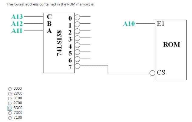
The lowest address contained in the ROM memory is: A13- A12- All C B 1 A10- El A 2 ROM 7 CS 0000 2D00 3C00 2С00 3D00 7D00 7C00 74LS138


Q: Memory cell is the basic element of a semiconductor memory and it can store one byte? O a. True b.…
A: Semiconductor memory is a semiconductor device which can store digital data. Major semiconductor…
Q: Q14: The arithmetic shifts right instruction ashr means divide the number by 2. Find the result of…
A: First 08 is loaded into the Acummulator in the form of binary. Given that ashr means divide the…
Q: AND/OR Gates Determine Vo for the given applied input voltages. Si E1 E2 Vo E1 1 OV O V Si E2 o Vo O…
A:
Q: how do i draw 2-3
A:
Q: Z1 ROMCS A YoO B YO Y2 O A16 A17 + RAMCS RESM* 22 dE YO Z3 Z4 A6 A Yo O RESP B YO- Y2 O OE Y O A7…
A: ROM INPUT OUTPUT 16 BITS
Q: input A to 1 and 0 and note the logic output
A: NOT Gate NOT gate is a Logical gate that acts as an inverter A Output 0 1 1 0
Q: The organization of a memory chip is 4KX8. How many bits wide is each memory location? 4 8 4K 32K
A:
Q: Q1) (1) If a RAM chip has n address input lines then it can access memory locations up to a) 2(n-1)…
A: We need to select correct option
Q: Part.5] Manually draw the implementation of the function Q = X+Y as logic circuit using 4xl…
A: A multiplexer is a device with several inputs and one outputs. It will select one input and forward…
Q: What are the contents of the ROM in as shown?(All FETs are NMOS.)
A:
Q: Q12/Assume that the microprocessor can directly address 1M with a and 8 data pins, The maximum RAM…
A: We need to find out maximum ram can be disign by using given chips .
Q: Computer M has 8-bit memory width with 8-bit address as illustrated in Figure Memory Memory Address…
A: An Big-endian or a little-endian are the two methods of storing data in the memory locations. In the…
Q: 20. In Figure 5, How many clock pulses are required to add two, 4 bit binary number ? Register B…
A: The given circuit diagram is
Q: A в- D Find the logic function of X *X = (A Ð B) + BC + C X = (AOB). B.C b. X = (AÐ B). B.C d. 'x =…
A: In this question we will find output of given function..
Q: Q3: The content of a four-bit register is initially the 4-bit word 0000. The register is shifted…
A: Given Serial input serial output ,four bit register initial value of 0000 The serial input is given…
Q: dout din ROM A0-A9 1KX8 cs By using above ROM and 3:8 decoder design memory of size 8KX8
A: Decoder circuit have more output than input. Decoder is combinational circuit that convert n bit…
Q: Q3) A- Convert the Excess-3 to binary number : (110001011100.10001010)ex-3 B- convert each Gray code…
A: Ex-3 nunber obtained by adding 3 to every digit of the decimal number
Q: Identify the logic of two voltage levels +6V and OV in a Positive logic system respectively. O Both…
A: Logic level morethan +5V is considered as logic 1,
Q: Q8/Assume that the microprocessor can directly address 64K with a R/W' and 8 data pins The memory…
A: solutin is on 2nd step
Q: A memory IC that can hold up to 1024 bits and has a 8 address lines can be organized into…
A: Answer: 256x4 a). It is not a valid option. 1024x1 requires 10 address lines. 210 = 1024. b) a).…
Q: 4 148+2816 = 3C16 5 Gray code representation of 1410 is 1010gray 6 The output of an AND gate will be…
A:
Q: 12/Assume that the microprocessor can directly address 1M with a and 8 data pins, The maximum RAM…
A: We need to find out total capacity
Q: 22) The 8-bit registers A, B, C & D are loaded with the value (F2) x (FF) he 39) hes hex and (EA)…
A: We are authorized to answer three subparts at a time, since you have not mentioned which part you…
Q: Difference between task and function in Verilog. What is Logic in system verilog.
A: Verilog is Hardware Description language . The memory and array declaration in Verilog is static…
Q: 3. Implement the following functions using a single 8 × 4 ROM. Use dot notation to indicate the ROM…
A: A ROM is a permanent memory. Its internal structure comprises two basic components: decoder and OR…
Q: write a sequence of instructions that stores a (33H) into 150h bytes of memory beginning at stack…
A: A data segment is a section of a program's virtual address space that holds the global and static…
Q: Write a sequence of instructions that stores a (33H) into 5 bytes of memory beginning at stack…
A: According to the question, we need to write an ALP to store 33 H into 5 bytes of memory beginning at…
Q: Part 2. Four Bit Wide 2 x 1 Multiplexer The combinatorial logic circuit for the half adder is shown…
A: As per the Bartleby guideline more than question askes only first to be answered. Please upload…
Q: EF - [X • (X•v]@(X+F) F = gr- (A+)-(A+C)]e[5•7-5)-(A•B•C)] F- [(4© B)• (A©C]•[(4+B+C)®(A•B•C]…
A: Solution- Given values for the variables are, X=0 Y=1 A=1 B=0 C=1
Q: RAM 이 256 X 4 A. The number 5 is being written to the memory at address location 203. B. The chip…
A: option A is not correct because the Address location is 211H not 203H. Option B is not correct…
Q: which of the following is incorrect regarding memory mapped I/O: a. Devices have 8-bit address line…
A: Memory mapped I/O : Address space provided both for memory and input output devices signal 1 or high…
Q: Implement the following functions using a single 8 × 4 ROM. Use dot notation to indicate the ROM…
A: Given: (a) W = A’B + B’C + AC’(b) X = AB’C + ABC’ + A’C(c) Y = A’C + AB’C’ + ABC(d) Z = A + B + C’…
Q: Which one is not a correct 8086 Assembly language instruction. a MOV (SI, CL b. MOV AX ISI) C MOV…
A:
Q: 2 docs.google.com Q جايتك The result of the following multiplication operation in number of base 13…
A:
Q: The capacity of a memory of is 14 KB, which is divided into two parts:cells with the addresses from…
A: 1) Registers ar a form of memory used to quickly settle for, store, and transfer knowledge and…
Q: Determine Vo for the given applied input voltages. Si E1 E2 Vo E1 DI O V ov O V Si E2 O V 10 V D2 10…
A: For the given positive logic OR gate, the output voltage V0 for the given applied input voltage is:
Q: Assume that the microprocessor can directly address 64K with a R/W' and 8 data pins The memory map…
A: Given: The microprocessor can directly address 64K with an R/W' and 8 data pins. To find: The memory…
Q: A fruit processing company wants to install an apple processing plant in Quetta. Company required…
A: Truth Table for the plant.…
Q: using Programmable Logic Devices (PLD ) requires More power supply Less power supply O None of them…
A:
Q: Explain the process of the following Load D3 · D3 12 12 D2 Do Clock D Load Block Diogram of 4-bit…
A: Given
Q: Q3. Perform the following: a. (6667)10 + (2598)10 using BCD b. Discuss floating point numbers by…
A:
Q: 6- Set BX to 4567H, CX to FEDCH and SP to A59FH, then run the instructions: PUSH BX PUSH CX a. What…
A: PUSH and POP can be used to save and restore the values of registers when the register needs to be…
Q: I have to draw a 2 logic circuits to implement the function F= A+BC+A'B' and the function G =…
A:
Q: Identify the true data dependencies, anti-dependencies, and output dependencies in the following…
A:
Q: 1. Construct a circuit whose output is X = A’C + BC +A’B’C, then draw the wiring diagram.
A: Logic Gates Logic gates are used as basic building blocks for implementing digital system. It is an…
Q: In the instruction MOV [BX+SI+BA H], DX the value present in DL will be stored in MA and the value…
A: To find out the correct answer
Q: 1. Debug program is an assembler to assemble the Mach. Lang. to Assemb. Lang. 2. LEA SI, [BX+DI]…
A: 1. Debug program is used for the conversion of the assembly language input to the machine language…


Trending now
This is a popular solution!

Step by step
Solved in 2 steps with 1 images


- Convert the following values to a 4-byte memory map assuming each is stored as an int : (a)(1AEEF5AA)base16 Byte Address In decimal Byte Value in hex (b)(1010100100010100001100011100110)base2 Byte Address In decimal Byte Value in hex (c)1073750032)base10 Byte Address In decimal Byte Value in hexGive addressing mode, number of bytes and function of following instruction in detail? a. LDA 3000H b. SUI 25H c. RRCquestion1:In a memory system, data is 16-bit wide. Break the information into bytes with their addresses using little endian and big-endian methods. Starting address is F800 and the data is: E0F2 0041 question2:What acknowledgment signals are there in I2C bus?
- Identify the contents of the registers, the memory location (C055H), and the flags as the following instructions are executed in 8085 microprocessor. A H L S Z CY M(C055H) LXIH, C055H MVI M,8AH MVI A,76H ADD M STA C055H HLTIf R0 = 0x20008000, after run STMDB r0!, {r3, r9, r7, r1, r2} command what is the r7 register memory start address?A. R0= 0x20007ff4B. R0 = 0x20007ffefC. R0 = 0x20007fffD. R0=0x20007fecE. R0 = 0x20007ff0What is the maximum memory size that can be connected to a processor with a lower order address bus of 24 lines and a higher order address bus of 4 lines? a. 256GB b. 16MB c. 256MB d. 16GB Note: Please do not handwritten.
- The processor has performed the following addition operation: 0x01A0+ 0xC410------0xC5B0 What decimal numbers did the processor add up, and what is the result of the addition if the programmer chose these numbers to be signed 16-bit number, where the lower four bits represent the fractional part of the number?Given a 8-bit number at memory location 2050H. Write 8085 instruction to move the value stored at the following locations: Register B Accumulator 2052H Write a single program and show register and accumulator screenshot and also attach memory view. In sim8085 software.DIsassemble the following MIPS 32-bit hexadecimal instruction written as addr:instr 60005000 : 0c000020
- Q. 1 There are different types of memories used in 8086 microprocessor one of them is called Stack. You are expected to investigate about it and answer the following questions related to it. i. What is stack memory? ii. What registers are associated with the stack in 8086? (including segment, pointer registers) iii. What is the use of stack? iv. Use any example which uses stack memory with appropriate instructions (PUSH, POP)Using 64×8 ROM chips with an enable input, construct a 512×8 ROM with eight chips and a decoder.How many bits are required to represent the Arduino analog input?Hint: There are 1024 possible values.Explain.