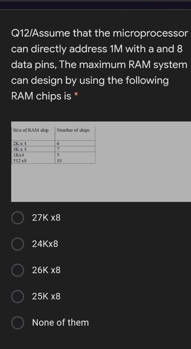
Q12/Assume that the microprocessor can directly address 1M with a and 8 data pins, The maximum RAM system can design by using the following RAM chips is Size of RAM chip Number of chips 2K x 4 4K x 4 6 7. 1KX4 512 x8 10 27K x8 24KX8 26K x8 25K x8 None of them
Q: In a microcomputer, the microprocessor unit (MPU) is always communicating with one of the following:…
A: 1. To activate the RAM step 1 address from A15 to A12 will pass through NAND gate and the input of…
Q: One of the following statement is not true about Registers of a microprocessor. a. Number of…
A: registers in the microprocessor are used to store the data
Q: 24) Specify the size of a single ROM that would be required to implement a 16-bit adder hubtractor…
A: According to the question we have to find size of single ROM.
Q: If a MOSFET is to be used in the making of logic gates application then it must work in O a.…
A: MOSFET should operate in cut-off and linear regions when used in logic gate applications. Because…
Q: d) Calculate the noise margin for a logic gate with the following logic levels: VIL = 1.0 V, VIH =…
A:
Q: The organization of a memory chip is 4KX8. How many bits wide is each memory location? 4 8 4K 32K
A:
Q: Q1) (1) If a RAM chip has n address input lines then it can access memory locations up to a) 2(n-1)…
A: We need to select correct option
Q: In the following statements one of them is not true O A sequence of microinstructions is called a…
A: The microprocessor is a processor embedded on a single chip, it performs all arithmetic logical, and…
Q: Q12/Assume that the microprocessor can directly address 1M with a and 8 data pins, The maximum RAM…
A: We need to find out total capacity for RAM capacity .
Q: The lowest address contained in the ROM memory is: A13- A12- All C B 1 A10- El A 2 ROM 7 CS 0000…
A: The explanation is as follows.
Q: Part.5] Manually draw the implementation of the function Q = X+Y as logic circuit using 4xl…
A: A multiplexer is a device with several inputs and one outputs. It will select one input and forward…
Q: true false the main concern of the memory interface are to connect 1/0 with buss
A: "Since you have posted a question with multiple sub-parts, we will solve first three sub-parts for…
Q: * 'Assume that the microprocessor can directly address 1M with a and 8 data pins, The maximum RAM…
A: We need to find out memory capacity for given chips
Q: Assume that the microprocessor can directly address 1M with a and 8 data pins. The maximum RAM…
A: Consider that the microprocessor can directly address 1M with a and 8 data pins. The maximum RAM…
Q: Results of arithmetic and logic instructions can be stored in one of two places. These are Program…
A:
Q: 2. It is the power available from power supplies that is consumed by the logic gate. 4. Identify the…
A: "Since you have posted multiple questions, we will solve the first one for you. To get the other…
Q: bit numbers and store lower byte of the result in accumulator A and higher byte in accumulator B.…
A: According to the question,
Q: dout din ROM A0-A9 1KX8 cs By using above ROM and 3:8 decoder design memory of size 8KX8
A: Decoder circuit have more output than input. Decoder is combinational circuit that convert n bit…
Q: Question 1: Use Indirect addressing to write a PIC24 assembly code that complements and adds 5 and…
A: Assembly language is nothing but a code for computer's understanding. To assign a particular task to…
Q: Q4:For the state diagram shown below write the state table and design logic circuit 0/0 001 0/0 1/1…
A: Present state Input Next state J2K2 J1K1 J0K0 Output Q2 Q1 Q0 X Q2* Q1* Q0* 0 0 0 0 0 1 1 0X 1X…
Q: Assume that 7 BCD data items are stored in RAM locations starting from 40 H. write an ALP to sum all…
A: MOV R0, #40H ; R0 is a pointer (memory location for BCD numbers) MOV R4, #0AH ; 7 iterations (Count…
Q: Design a memory of size 8KX8 using a 3:8 decoder and the minimum number of ROMS of size 1KX8 shown…
A: Decoder circuit have more output than input. Decoder is combinational circuit that convert n bit…
Q: 2- Which of the following instruction cannot be coded in 8086 assembly language "give the reason why…
A: A symbol of the code needed to program an explicit electronic equipment design is enforced in the…
Q: A ROM chip with a 128Kx8 organization has _______ memory locations.
A:
Q: The Example of 32 bit Intel microprocessor are : O Non of them 80286, 80386, 80486 Intel® Core™ i5,…
A: The bit of given processor are shown in table below, Processor CPU Bit 80286 16-bit 80386…
Q: 12/Assume that the microprocessor can directly address 1M with a and 8 data pins, The maximum RAM…
A: We need to find out total capacity
Q: What is it: Microprocessor/Cache Memory/SRAM/DRAM/EPROM Vce - Vss 23 D3 22 D2 How many addressable…
A: Soluiton a) Since it has 24 pins ,This structure is called 16mb (4MBx4)It has memory package and…
Q: w is an NMOS logic circuit. For all of the MOSFETs assume V th 5V 5V R₂ = 5600 R₁ = 4700 M3 Vo
A:
Q: 4. Show how to connect two of the 6264C RAM chips symbolized in the figure below to produce a 16K X…
A: Given: The 6264C RAM chips symbolized in the figure below to produce a 16K X 8 RAM module. The…
Q: QI) What is the result of executing the following sequence of instructions? MOV AL, 99 MOV BL, IBH…
A: The solution can be achieved as follows.
Q: 4- Find the result in the memory location 2002 H after the following programs implemented: MVI A, 1F…
A: The solution can be achieved as follows.
Q: 2. The Illogic Company has developed a new logic family which has the following characteristics: VOH…
A: A group of logic circuits built with power supply and compatible logic levels known as a Logic…
Q: Q1) Draw the ladder diagram for the logic circuits A&B В: S* (M+W) = (S*W)HS*M) W (M+W) M A
A:
Q: I need help drawing the logic gate path for this equation AB + ACD(AFR + ABC + A) + DFE + A'B + AB'
A: The given expression is as shown below, AB + ACD(AFR + ABC + A) + DFE + A'B + AB'
Q: A microprocessor that performs subtraction with complementary arithmetic; What value does the result…
A: A microprocessor that performs subtraction with complementary arithmetic;What value does the result…
Q: which of the following is incorrect regarding memory mapped I/O: a. Devices have 8-bit address line…
A: Memory mapped I/O : Address space provided both for memory and input output devices signal 1 or high…
Q: Which one is not a correct 8086 Assembly language instruction. a MOV (SI, CL b. MOV AX ISI) C MOV…
A:
Q: How many addresses are there in a 16M x 8 ROM chip? 16M 23 21 24 13 11 14 8
A: 16M x 8 General formula to find out ROM memory size is 2mxn, where m is address lines and n is data…
Q: Design a Circuit to perform the following Operation.
A: Break the A+B-C operation in two parts as: A+B=S S-C For First Operation, Take Half adder to…
Q: Assume that the microprocessor can directly address 64K with a R/W' and 8 data pins The memory map…
A: Given: The microprocessor can directly address 64K with an R/W' and 8 data pins. To find: The memory…
Q: using Programmable Logic Devices (PLD ) requires More power supply Less power supply O None of them…
A:
Q: How can I create a circuit based on the table below, I have 2 inputs and 2 outputs. I would like to…
A:
Q: (a) Digital Conversion, Sampling and Computer Architecture ADC RAM DAC DDR CPU ROM BIOS EDC (i)…
A: “Since you have asked multiple question which are not interlinked with each other , we will solve…
Q: In a microcomputer, the microprocessor unit (MPU) is always communicating with one of the following:…
A: According to the question, we need to determine the range of address A15 to A8 that will activate…
Q: B- Write an 8086 assembly language program to find the highest grade of five people with the…
A: Program to find the highest grade of five people with the following grades: 69, 87, 96, 45 and 75.…
Q: Q3/Assume that the microprocessor can directly address 64K with a and 16 data pins The memory map…
A:
Q: A Programmable Logic Device (PLD) is an integrated circuit with internal logic gates that are…
A: we need to find that in a Programmable Logic Device (PLD) is an integrated circuit with internal…
Q: Q 1. (a) Specify the memory location and its contents after the following instructions are executed.…
A: The instruction given in the problem is executed as below, MVI B, F7H Hexadecimal data F7H is…
Q: 39 - What advantage does the simplification of logic circuits provide from the following? A) All…
A: Advantages of logic simplification are listed below:
Step by step
Solved in 2 steps with 1 images
- Microprocessor , For a data segments for an 8086 µP memory system has 64 kB size, with segment address is 1234 H. Find the offset for a memory address 125FC H.1. Design 8086’s memory system consisting of 64K bytes of ROM using32KX8 chip. The memory is to reside over the address range 60000Hthrough 6FFFFH. Select suitable address maps.2. If the memory chip size is 1024 X 4 bits, how many chips are required tomakeup 2K bytes of memory?3. Interface 16 K word of memory to the 8086-microprocessor system.Available memory chips are 8 K X 8 RAM. Draw the memory table.Draw pinouts of 8088 or 8086 microprocessor (μp). Also draw schematics of 8088/8086 μp buses with Latch(s) [IC: 74LS373] and Buffer(s) [IC: 74LS245]. Write purpose of using latch and buffer ICs with μp buses. Please Answer all parts
- What is the starting and ending address of a 256K x 8 memory? How many address lines will be required to interface this memory with 8086? Also, draw the interfacing diagram with 8086You buy a ROM memory chip that is 64Kx8. How many memory address lines does the chip have? A 16 B 64K C 512 D 8Give the logic diagram of half subtractor. NOTE: SUB: DIGITAL LOGIC AND DESIGN(DLD) DEPTT:CS/IT.
- What is the total capacity in hexadecimal representation for any segment base address wtihin the 8086 microprocessor's real address mode RAM?-FEFFh-BHAFh-FFFFh-EEEEhIn fully buffered 8088, it requires __ number of 74LS245. Solve the MCQ no need for explanation. Book Reference Barry B Brey 8th edition.1. What is the total or equivalent resistance of ten (10) nos of 10-ohm resistors connected in parallel? 2. A single logic gate in a prototype integrated circuit is found to be capable of switching from the “on” state to the “off” state in 12 ps. This corresponds to: a. 1200ns b. 1.2 ns c. 12000 ns d. 120 ns
- Solve in 8086 microprocessorUsing a single 7400 IC, construct a circuit to output the following Boolean function: F = A B + C DA certain packaged IC chip can dissipate 5W. Supposewe have a CMOSIC design that must fit on onechip and requires 10 million logic gates. What is theaverage power that can be dissipated by each logicgate on the chip? If the average gate must switch at100 MHz, what is the maximum capacitive load ona gate for VDD =3.3 V, 2.5 V and 1.8 V.