1. Bus system that reads 2 registers at the same time, where the total number of registers is six registers(A,B,C,D,E, and F), and the size of each register is 5 bits.
1. Bus system that reads 2 registers at the same time, where the total number of registers is six registers(A,B,C,D,E, and F), and the size of each register is 5 bits.

Database System Concepts
7th Edition
ISBN:9780078022159
Author:Abraham Silberschatz Professor, Henry F. Korth, S. Sudarshan
Publisher:Abraham Silberschatz Professor, Henry F. Korth, S. Sudarshan
Chapter1: Introduction
Section: Chapter Questions
Problem 1PE

Related questions
Question
I need the answer as soon as possible
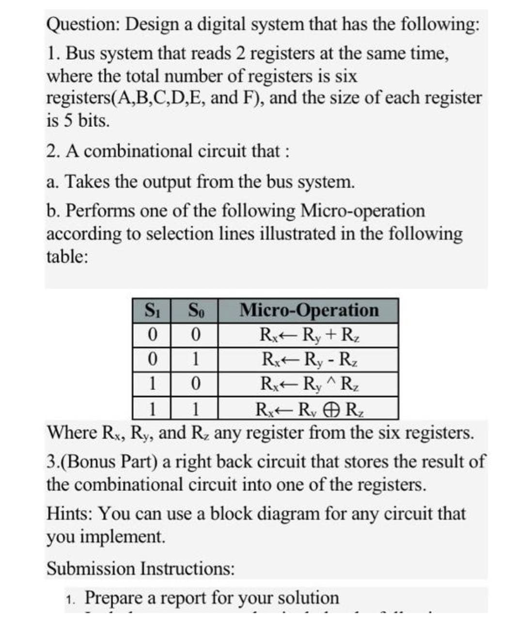
Transcribed Image Text:Question: Design a digital system that has the following:
1. Bus system that reads 2 registers at the same time,
where the total number of registers is six
registers(A,B,C,D,E, and F), and the size of each register
is 5 bits.
2. A combinational circuit that:
a. Takes the output from the bus system.
b. Performs one of the following Micro-operation
according to selection lines illustrated in the following
table:
Si
Micro-Operation
R-Ry + R,
R Ry- R2
R Ry ^Rz
R R, OR,
Where Rx, Ry, and R, any register from the six registers.
So
1
1
1
1
3.(Bonus Part) a right back circuit that stores the result of
the combinational circuit into one of the registers.
Hints: You can use a block diagram for any circuit that
you implement.
Submission Instructions:
1. Prepare a report for your solution
Expert Solution
This question has been solved!
Explore an expertly crafted, step-by-step solution for a thorough understanding of key concepts.

This is a popular solution!

Trending now
This is a popular solution!

Step by step
Solved in 2 steps with 1 images

Recommended textbooks for you
Database System Concepts
Computer Science
ISBN:
9780078022159
Author:
Abraham Silberschatz Professor, Henry F. Korth, S. Sudarshan
Publisher:
McGraw-Hill Education

Starting Out with Python (4th Edition)
Computer Science
ISBN:
9780134444321
Author:
Tony Gaddis
Publisher:
PEARSON

Digital Fundamentals (11th Edition)
Computer Science
ISBN:
9780132737968
Author:
Thomas L. Floyd
Publisher:
PEARSON
Database System Concepts
Computer Science
ISBN:
9780078022159
Author:
Abraham Silberschatz Professor, Henry F. Korth, S. Sudarshan
Publisher:
McGraw-Hill Education
Starting Out with Python (4th Edition)
Computer Science
ISBN:
9780134444321
Author:
Tony Gaddis
Publisher:
PEARSON
Digital Fundamentals (11th Edition)
Computer Science
ISBN:
9780132737968
Author:
Thomas L. Floyd
Publisher:
PEARSON

C How to Program (8th Edition)
Computer Science
ISBN:
9780133976892
Author:
Paul J. Deitel, Harvey Deitel
Publisher:
PEARSON

Database Systems: Design, Implementation, & Manag…
Computer Science
ISBN:
9781337627900
Author:
Carlos Coronel, Steven Morris
Publisher:
Cengage Learning

Programmable Logic Controllers
Computer Science
ISBN:
9780073373843
Author:
Frank D. Petruzella
Publisher:
McGraw-Hill Education