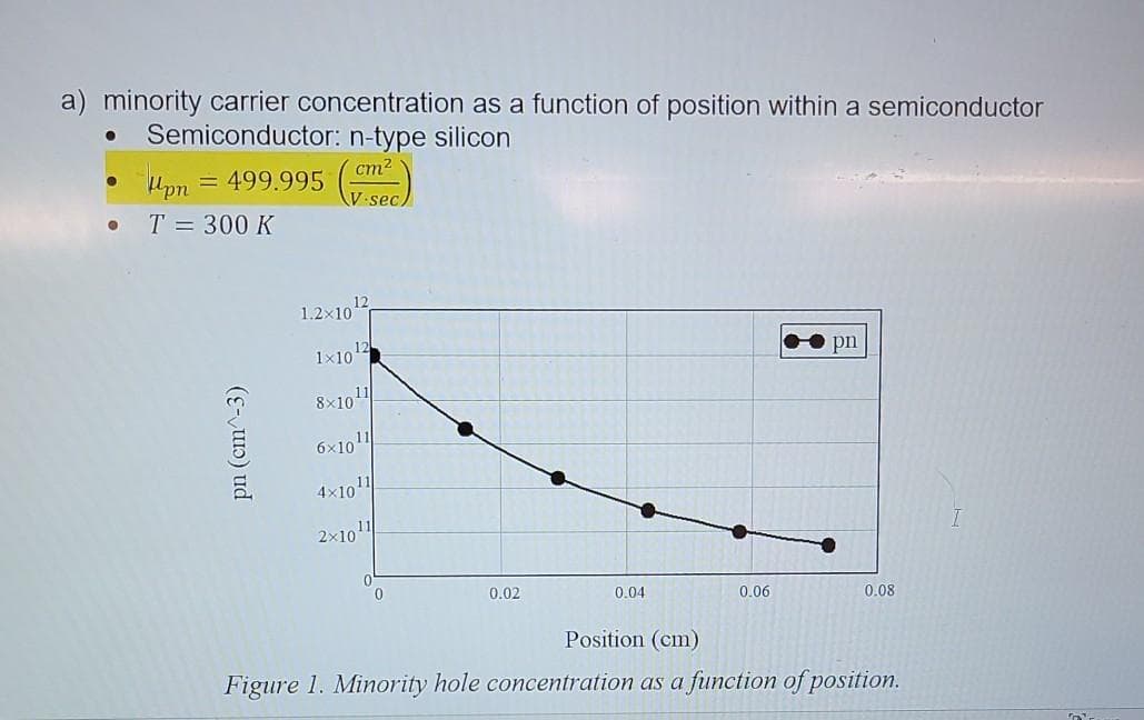
12 1.2x10 12 1x10 pn 8x101 6x10" 11 4x10 2x10 0.02 0.04 0.06 0.08 Position (cm) pn (cm^-3)


Q: F. Use this graphic for Question 6. R1 A 2 kQ R2 5 kQ B vs 35 V 34 kQ R3 3 ko
A:
Q: 71, – 212 – 313 = 8 → Eq. 1 -21, + 712 – 313 = 8 → Eq. 2 -4 - 12 + 313 = 0 → Eq. 3 Answer: I =…
A:
Q: Draw the voltage vm as a function of time when Zo = Ro = 500 for figure shown www 5002 S3 10002…
A: In this question we need to draw the voltage Vm as a function of time
Q: A1 B1 A0 Во- F X1
A:
Q: 0-08905 14.67V Om Cable resistance 12.523 1-74A 7.15V 2072 (1)6.67A
A:
Q: What is the voltage across R1?
A: To find the voltage across resistance R1 in the circuit
Q: Question 16 Determine the total current on a circular wire of radius 4mm and J =500a, A/m2 1.57 mA…
A: Given Current density find current value
Q: A Moving to another question will save this response. uèstion 13 Determine the total current on a…
A: In this question we will find total current due to circular wire...
Q: BlAck Box 1. Una caja negra conteniendo un circuito se conecta a un resistor variable. Se miden el…
A:
Q: 92 Fuind a12= In /Ia Iz /I1 %3D 2 Ia 2173. I, (1 312
A:
Q: 10.Calculate the amount of charge represented by 4600 electrons. A. +7.408 • 10-13. B. -7.36*…
A: Given, 4600 electrons To calculate the total amount of charge-?
Q: SPheres hauesta conducting charges .147 pC an T.851 pC sthy are two Hentiaal Conduc tiy Brought Ynto…
A: In this question we are given two charges . And when they came in contact , the charge is…
Q: Q1) Plot the following functions on the same plot where 0<x<4 with 0.1 as increment: (1) f(x) = nx…
A:
Q: E. Use this graphic for question 12 L1 L3 3mH 5mH L2 6mH
A: The solution is given below
Q: Take a graph sheet and divide it into 4 equal parts. Mark origin at the center of the graph sheet.…
A: The diodes are made of semiconductor materials. Silicon and germanium are common semiconductors for…
Q: 2. Determine whether or not each of the following systems goe time verriant i) yon] = x0] – x[n-] or…
A:
Q: Q3/ Find the difference equation from this block diagram below: x(n) y(n) z-1 22- -3 3.
A:
Q: x(t) 1 T 2T 3T 4T 5T h:(t) 1- T 2T
A: The expression for the convolution theorem is given by: xt*h1t=∫-∞∞xτh1t-τdτ For t>-T, the…
Q: 3.) Given Qo = 500µC with the displayed polarity, and that the switch closes at t = 0 s, find: a.)…
A:
Q: Jhwot dt -011
A: In this question, We need to determine the value of Fourier series representation of the given…
Q: Q2/ Determine the horizontal resultants about A knowing that point A is fixed support taking * .e=45…
A:
Q: 32K×4 A14 En • CS
A:
Q: Refer to the Graphic B. What is the current through R1? 5.34 mA O 2.73 mA 6.23 mA 3.90 mA None of…
A: Option a 5.34 mA Ue basic ohms law Current = voltage / resistance Here current through R1 is the…
Q: 0.04div (2.5MS/s) M:200us 0.00mV 22y- 0.0041s7 Donth 1o
A: Red Signal
Q: 4- (1111001 + 1011 )2 = (X)2 5- (- 14 )10 - (-13 )10 = (x)2 6 - (1010101010) Gray (X)2 using 2's…
A:
Q: Question 23 x. R1 Vs R2 3 C0 Vs = 24V R1 = 1Kohms R2 2 Kohms C-4uF. At t-0 the switch is opened. The…
A:
Q: Simplify the following using K-map: a) Y = W'XYZ + WX'YZ + WYZ+X'YZ
A: In this question we use k map to simplify the given Boolean expression
Q: For which measurement is this oscilloscope time difference reading useful? Oscilloscope-XSC1 Time…
A: By using time difference,
Q: C. Perform the indicated operations (b) 13– 4i || 4+ 3i l:
A:
Q: Determine R1 TO R5 V1 TO V5 I1 TO I5 R TOTAL
A: Write the values of all the resistances as given in the figure. R1=2.2 kΩR2=4.7 kΩR3=470 ΩR4=1…
Q: DC Voltage has ______ polarity
A: Dc voltage has single polarity.
Q: Calculate enersy x[n]: +3] In-
A: Energy of discrete time signal can be defined by the formula Energy signals are absolutely summable…
Q: Find 2: +1 (z+ 1)(z - 3)
A:
Q: In order to select the chip shown, A19-A14 must be set to B A13 A0 A19 32K×4 A14 En A15 CS 1011 0B…
A: In the chip circuit, the enable pin (En) is active high enable which means “1” is given to the…
Q: Q1/ check the signal below : (energy or power) X(t) = e2at u(-t) *
A:
Q: (a) (b) (c) (d) If you will inspect the trend of the following situations, going from left to right…
A: Accuracy and precision both are the parameters of measuring any values. Accuracy mean the closeness…
Q: Question 2: (do yoursel} ) Deteimine CuIrent when t:0 in the cPreuit shown in bigure below using…
A: Circuit is given as,
Q: In order to select the chip shown, A19-A14 must be set to A13 A0 A19 32K×4 A14 En A15 CS 1011 O B…
A: NAND gate is known as Universal gate. NAND gate gives high output if any of the input is low and it…
Q: ARROWHEAD 35mm 7.0 В D HIDDEN LINE- 3mm K 015 1. NOTE Smm H. E. AB
A: Line B is generally mentioned as the Extension line .
Q: Find i 4i1 2Ω 5 V + 3 V 4Ω.
A: according to the question we need to calculate the value of i1.
Q: Question 26 Determine VTH when R₁ is 180 and X₁ is 90. R1 90 Ω VS RL 30/0°V 12.220° V —00000) +1₁ XL…
A: In this question we will find thevein voltage....
Q: Find the inverse DTFT of X(ejo): = 1- 13 12 13 e-jo +2 -jw e 12 + 1 4 e-2 joo
A:
Q: Dawvre, avve, Suppose you have two point charges each of 79 nC. Ananya Ananya daveicloud.com xpertta…
A: The value of the first charge is, q1=79 nC The value of the first charge is, q2=79 nC Since the…
Q: Q1/ check the signal below : (energy or power) X(t) = e2at u(-t)
A:
Q: Pale map 3. T.F. S+s+2 Plat zevo -
A: In this question we need to plot a zero - pole map of the given transfer function.
Q: X(s) Y(s) B D F H G five loops and three forward paths
A: The forward paths in the block diagram are: F1 : ABD F2 : AJH F3 : ABCBD F4 : EFH F5 : EFGFH F6 :…
clear and correct or dislike
explain to me what is happening on this graph? Full detail

Step by step
Solved in 2 steps

- Boron gas is used to dope the silicon wafer to a dopant concentration of 10¹6 / cm³. After letting the sample cooldown to 300K (a) What is the new number of free electrons and holes in equilibrium? (b) What type of semiconductor do we have after the process?Calculate the intrinsic carrier concentration of a semiconductor in units of (cm-3). Use the room temperature bandgap and effective density of states. Assume the parameters given below: Semiconductor: Germanium Temperature: 206 (K)Estimate the amount of free electrons and holes in a N-doped Silicon wafer a) at room temperature with 1014 cm-3 doping level, and b) at 650K with 1015 cm-3 doping level
- Assume D = D0e^–Ea/kT is the diffusion coefficient of boron in silicon surface, whereD0 = 10.5 cm^2/s and Ea = 3.7 eV. The substrate is N-type silicon doped to 10^15 cm^3.N0 = 10^15 cm^2 of boron is introduced just below the silicon surface.(a) What is the junction depth after a 1-h drive-in at 1,100°C?(b) By how much will the junction depth change after 10^6 h (~100 years) of operation at100°CA silicon diode is in connected to a DC voltage source with Forward biased, the net currentflowing through the diode is (25mA) where the applied voltage across the terminals of thediode is (820mV). Determine diode temperature, if Is "dark saturation current", the diodeleakage current density in the absence of light is 3.4 × 10⁻¹⁰ AThe applied electric field in p-type silicon is E=10V/cm. The semiconductor conductivity is 1.5(Ω-cm)-1and cross-sectional area is 10-5cm2. Determine the driftcurrent. (b) A drift current density of 120A/cm2is established in n-type silicon with an applied electric field of 18V/cm. If the electron and hole mobilities are µn =1250 cm2/V-s and µp =450 cm2/V-s, respectively, determine the required doping concentration.
- A particular semiconductor is doped at ND=8xl0l6 cm-3 and NA=2xl0l6 cm-3 and ni=1010 cm-3. Assume complete ionization. Determine thermal equlibrium concentrations of majority- and minority-carrier concentrations. Lütfen birini seçin: Majority carrier; no= 8xl0l6 cm-3 Minority carrier; po = 1250 cm-3 Majority carrier; no = 6xl0l6 cm-3 Minority carrier; po = 1666 cm-3 Majority carrier; no= 2xl0l6 cm-3 Minority carrier; po = 5000 cm-3An n-type semiconductor with direct band structure (Eg = 2.5 eV) is applied with a DC voltage shown below. (i) Schematically draw the band diagram for this semiconductor under this DC voltage. (ii) Calculate the longest wavelength in light absorption from this n-type semiconductor with applied DC voltage.A diode has wdo = 1.5 μm and φj = 0.8 V. (a) What is the depletion layer width for VR =5V? (b) For VD = −10 V?
- Consider the diode circuit shown below. If Vs is a sinewave with a peak amplitude of 12 Volts at 60Hz, and diodes D1 & D2 are considered ideal, sketch the appearance of the waveform at node voltage Vout . Sketch the appearance of the waveform at Vout .Elaborate the following with Scientific Reason a. Why Intrinsic Semiconductor materials are the bad conductors of electricity? Elaborate the process to make them full conductors b. Elaborate the concept and importance of Majority Carriers and Minority Carriers inside P-N Junction c. Elaborate why Depletion Zone inside P-N Junction is a problematic area? What necessary measurement should be taken to remove the depletion zone?An intrinsic semiconductor with an intrinsic hole concentration of pi = 1.45x10^10/cm^3, has been doped with a trivalent atom generating a majority hole concentration of pp = 20^20/cm^3. Find the resulting minority carrier concentration.