2a) Design a logic circuits that has three inputs As,A2 and Ao and some select and enable inputs so that it functions according to the requirement given below: So Ao 1 As A2 Construct a 4X16 decoder using 3-to-8 Decoders. 1 2b)
2a) Design a logic circuits that has three inputs As,A2 and Ao and some select and enable inputs so that it functions according to the requirement given below: So Ao 1 As A2 Construct a 4X16 decoder using 3-to-8 Decoders. 1 2b)

Chapter22: Sequence Control
Section: Chapter Questions
Problem 6SQ: Draw a symbol for a solid-state logic element AND.

Related questions
Question
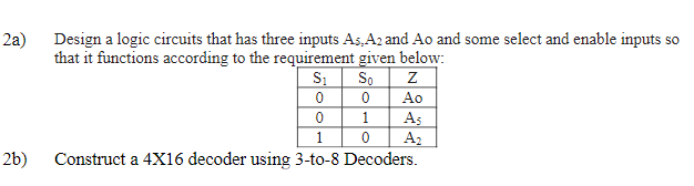
Transcribed Image Text:2a)
Design a logic circuits that has three inputs As, A2 and Ao and some select and enable inputs so
that it functions according to the requirement given below:
So
Ao
1
As
A2
1
2b)
Construct a 4X16 decoder using 3-to-8 Decoders.
Expert Solution
This question has been solved!
Explore an expertly crafted, step-by-step solution for a thorough understanding of key concepts.

Step by step
Solved in 3 steps with 3 images

Knowledge Booster


Learn more about
Need a deep-dive on the concept behind this application? Look no further. Learn more about this topic, electrical-engineering and related others by exploring similar questions and additional content below.Recommended textbooks for you