Q2. Minimize the combinational logic circuit in the following figure using Karnaugh's map only. Inverters for the complemented variables are not shown.
Q2. Minimize the combinational logic circuit in the following figure using Karnaugh's map only. Inverters for the complemented variables are not shown.

Chapter22: Sequence Control
Section: Chapter Questions
Problem 6SQ: Draw a symbol for a solid-state logic element AND.

Related questions
Question
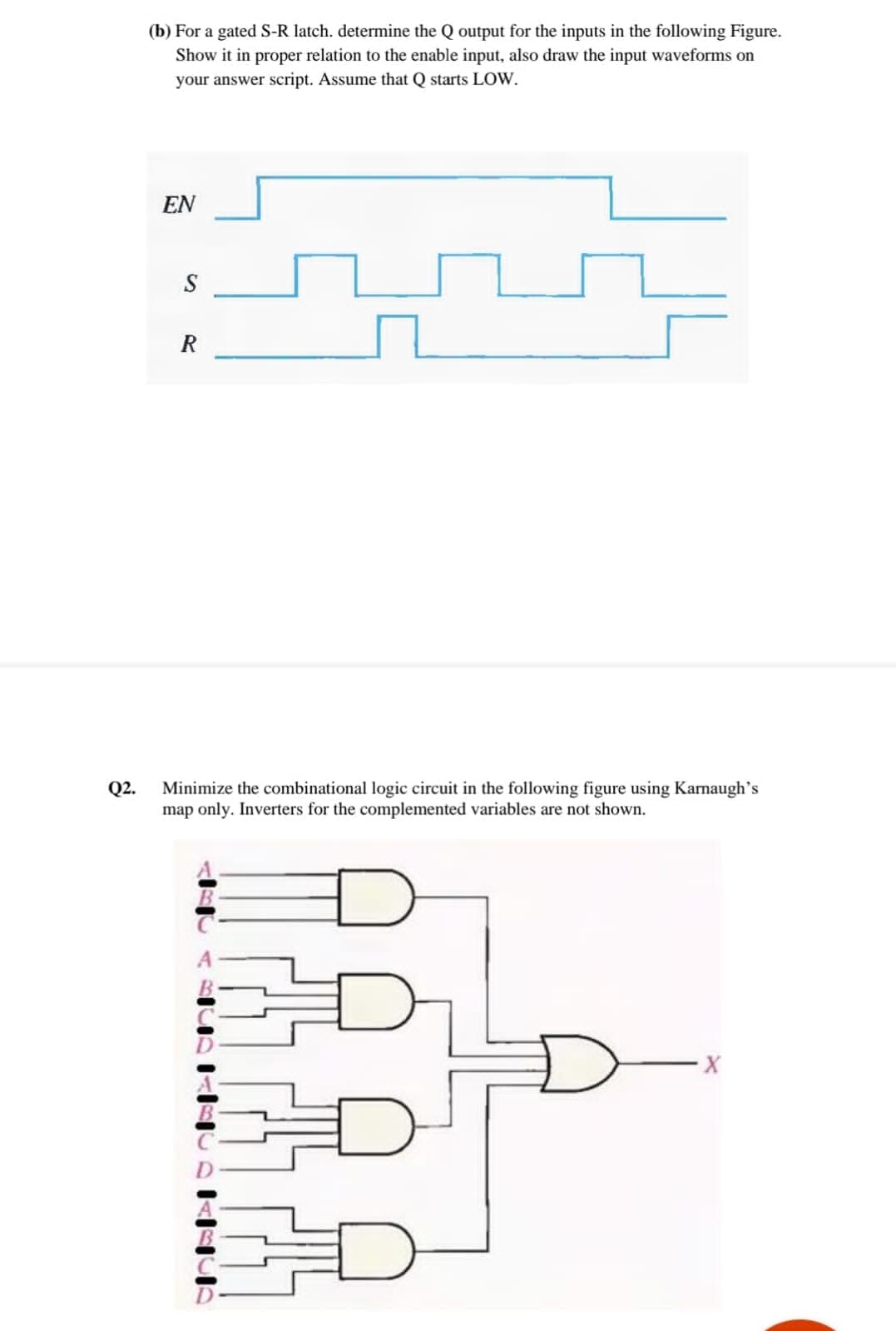
Transcribed Image Text:(b) For a gated S-R latch. determine the Q output for the inputs in the following Figure.
Show it in proper relation to the enable input, also draw the input waveforms on
your answer script. Assume that Q starts LOW.
EN
S
R
Minimize the combinational logic circuit in the following figure using Karnaugh's
map only. Inverters for the complemented variables are not shown.
Q2.
Expert Solution
This question has been solved!
Explore an expertly crafted, step-by-step solution for a thorough understanding of key concepts.

This is a popular solution!

Trending now
This is a popular solution!

Step by step
Solved in 2 steps with 2 images

Knowledge Booster


Learn more about
Need a deep-dive on the concept behind this application? Look no further. Learn more about this topic, electrical-engineering and related others by exploring similar questions and additional content below.Recommended textbooks for you