3. Describe the fundamentals of the use in the pn junction diode, LED and resistor in each of the digital block design. Adopt constant voltage drop (CVD) model in analyzing and describing the operation of the diode. 4. Utilizing PSPICE/LTSPICE, construct the circuit architecture. Simulate the testbench as illustrated in Figure 2 with random bit sequence at the input in time domain. 5. Extract the transient output in each logic blocks and explain quantitatively/qualitatively the discrepancy between an ideal logic gate output and the implemented diode-diode logic output. 6. The first page of the report should be attached with the assessment rubric given in the
3. Describe the fundamentals of the use in the pn junction diode, LED and resistor in each of the digital block design. Adopt constant voltage drop (CVD) model in analyzing and describing the operation of the diode. 4. Utilizing PSPICE/LTSPICE, construct the circuit architecture. Simulate the testbench as illustrated in Figure 2 with random bit sequence at the input in time domain. 5. Extract the transient output in each logic blocks and explain quantitatively/qualitatively the discrepancy between an ideal logic gate output and the implemented diode-diode logic output. 6. The first page of the report should be attached with the assessment rubric given in the

Chapter22: Sequence Control
Section: Chapter Questions
Problem 6SQ: Draw a symbol for a solid-state logic element AND.

Related questions
Question
Transcribed Image Text:3. Describe the fundamentals of the use in the pn junction diode, LED and resistor in
each of the digital block design. Adopt constant voltage drop (CVD) model in analyzing
and describing the operation of the diode.
4. Utilizing PSPICE/LTSPICE, construct the circuit architecture. Simulate the testbench
as illustrated in Figure 2 with random bit sequence at the input in time domain.
5. Extract the transient output in each logic blocks and explain quantitatively/qualitatively
the discrepancy between an ideal logic gate output and the implemented diode-diode
logic output.
6. The first page of the report should be attached with the assessment rubric given in the
attachment, followed by the complete report.
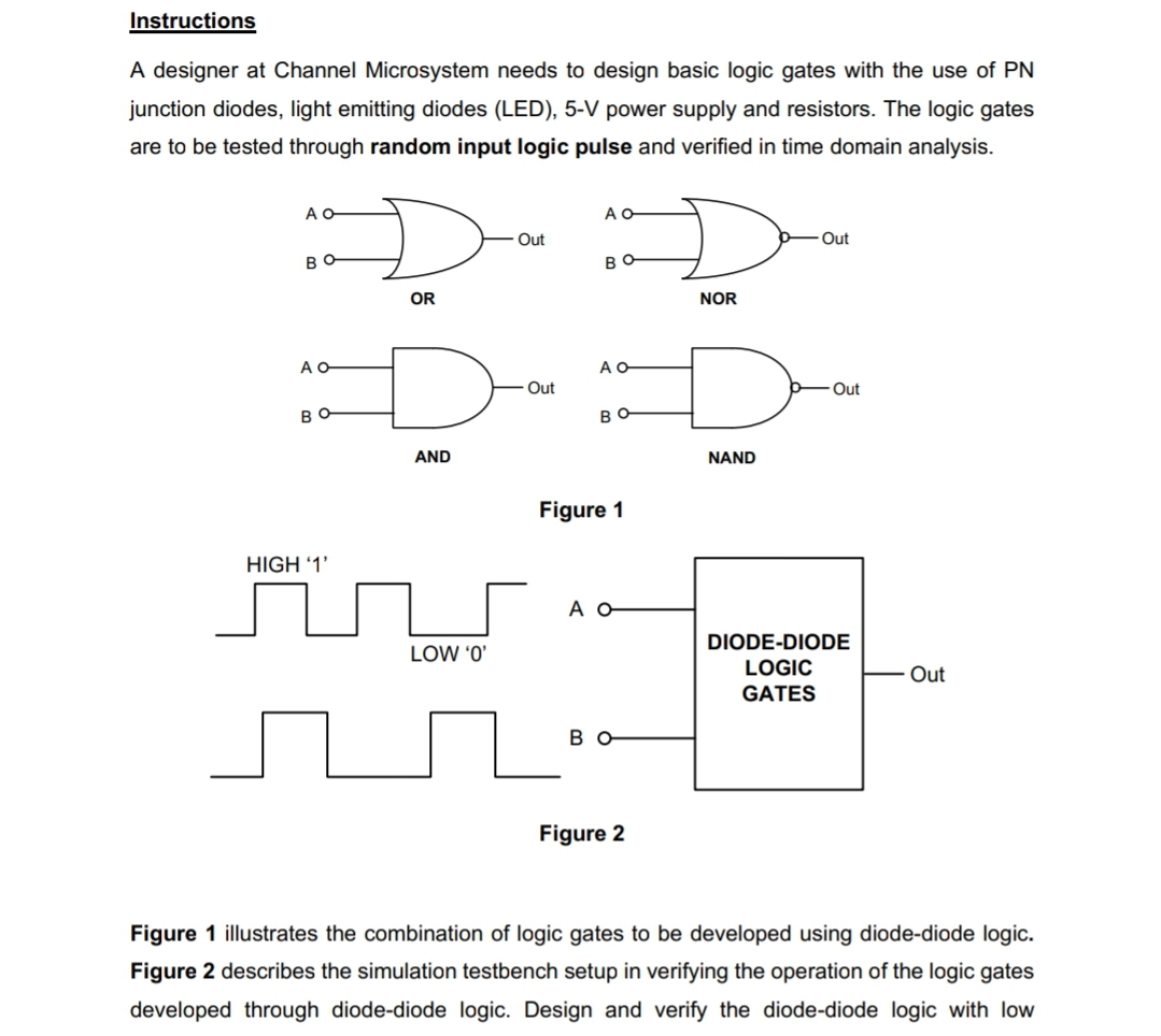
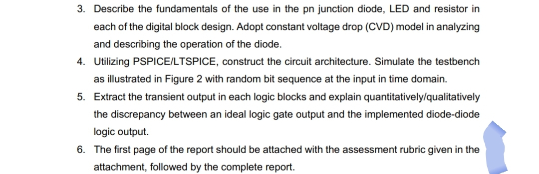
Transcribed Image Text:Instructions
A designer at Channel Microsystem needs to design basic logic gates with the use of PN
junction diodes, light emitting diodes (LED), 5-V power supply and resistors. The logic gates
are to be tested through random input logic pulse and verified in time domain analysis.
A O
A O
Out
Out
BO
BO
OR
NOR
A O
Out
Out
BO
в о
AND
NAND
Figure 1
HIGH '1'
DIODE-DIODE
LOW '0'
LOGIC
Out
GATES
во
Figure 2
Figure 1 illustrates the combination of logic gates to be developed using diode-diode logic.
Figure 2 describes the simulation testbench setup in verifying the operation of the logic gates
developed through diode-diode logic. Design and verify the diode-diode logic with low
Expert Solution
This question has been solved!
Explore an expertly crafted, step-by-step solution for a thorough understanding of key concepts.

Step by step
Solved in 4 steps with 4 images

Knowledge Booster


Learn more about
Need a deep-dive on the concept behind this application? Look no further. Learn more about this topic, electrical-engineering and related others by exploring similar questions and additional content below.Recommended textbooks for you