Q1 Write the difference between TTL and CMOS logic families according to the following table: SPECIFICATION TTL СMOS Components Basic Gate Noise Immunity Fan-out tp in ns Noise Margin Power/gate in mWatt Figure of Merit
Q1 Write the difference between TTL and CMOS logic families according to the following table: SPECIFICATION TTL СMOS Components Basic Gate Noise Immunity Fan-out tp in ns Noise Margin Power/gate in mWatt Figure of Merit

Chapter22: Sequence Control
Section: Chapter Questions
Problem 6SQ: Draw a symbol for a solid-state logic element AND.

Related questions

Question
100%
TAPLE ANSWER?
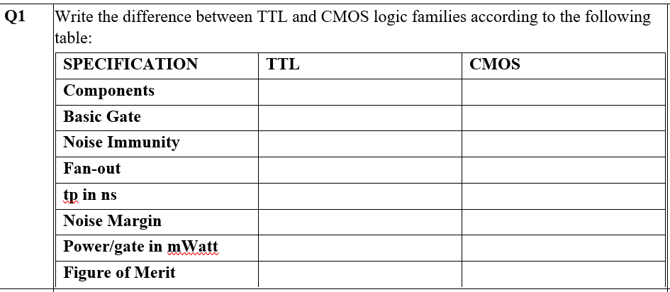
Transcribed Image Text:Write the difference between TTL and CMOS logic families according to the following
table:
Q1
SPECIFICATION
TTL
СМOS
Components
Basic Gate
Noise Immunity
Fan-out
tp in ns
Noise Margin
Power/gate in mWatt
Figure of Merit
Expert Solution
This question has been solved!
Explore an expertly crafted, step-by-step solution for a thorough understanding of key concepts.

Step by step
Solved in 2 steps with 1 images

Knowledge Booster


Learn more about
Need a deep-dive on the concept behind this application? Look no further. Learn more about this topic, electrical-engineering and related others by exploring similar questions and additional content below.Recommended textbooks for you