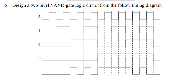
5. Design a two-level NAND-gate logic circuit from the follow timing diagram %3D %3D %3D %3D


Q: Construct the circuit using RTL (resistor transistor logic) components for the function;…
A: Given that : F(A,B,C,D)=∑(0,4,8,12,14). First we will simply the sop expression using k map. Then we…
Q: 3) a) What is the logic function that is implemented by the gate in the below figure? b) What are…
A:
Q: Which of the following logic valve is known as shuttle valve? O a. NOR gate O b. OR gate O C. AND…
A: i have explained in detail
Q: H.W. for Bipolar +Ao logics → Am -A togico→-Aen Vth ?? frove
A: prove pc=Q(Aσn)=Q(SNR)
Q: ülebäi The logic circuit represented by the figure shown below is A Doz B OR O AND O NAND O NOR O
A:
Q: 4. In the logic circuit shown below, what is the minimum RL that the inverter drive without causing…
A:
Q: A B 2
A: The given data is as follows:-
Q: 1.) Using internet (google) or Textbook or Reference book of Digital Electronics, Determine the…
A: (a) 3-INPUT NAND GATE: The 7400 series of logic ICs is a well-liked set that can be obtained from a…
Q: 2. Implement the logic function G(A, B, C) = (B+ C)(Ā + B)(A + B + T) using the following Decoder…
A: A combinational circuit is one in which the various gates in the circuit, such as the encoder,…
Q: Draw the logic diagram for the following functions, then map it using NAND only technology and NOR…
A:
Q: Realize the function f(a, b.c,d) = Em(13462.11.12.14) (Fonksiyonu gerçekleyiniz!) (a) Use a single…
A:
Q: Given the logic expression: Y=A+BC+ABD+ABC 1-Express it in standard SOP form 2-Draw K-map and…
A: Given logical expression, Y=A+B¯ C¯+ABD¯+ABCD. Some Boolean properties are mentioned below which can…
Q: V dd Q1 Q2 Q5 Q3 A - Output Q4 Q6 B Write down the truth table for above logic gate with the ON /…
A:
Q: Speed Power Product (SPP) is a figure of merit of a logic circuit which is based on the product of…
A: speed power product = propagation delay(ns)* power dissipation(mW) power dissipation = voltage *…
Q: Assume that you need 0.6 V across RE to properlystabilize the current in the modified ECL gateas…
A: Given logic swing = 0.4 V, average current = 1 mA. Calculating voltage at low logic level…
Q: Apply Karnaugh map to design a logic gates circuit for the following conditions : a- When the input…
A:
Q: Given the expression F = A’B + CD + {(A+B)’ [(ACD) + (BE)’]} ,draw its logic implementation using…
A:
Q: Draw a demultiplexer using only NAND gates and inverter gates. Give a detailed explanation of the…
A: A combinational circuit is one in which the various gates in the circuit, such as the encoder,…
Q: Q.4 Draw the logic diagram to implement the following expression with minimum number of NAND gates.…
A: The solution is provided in the following section:
Q: Implement using full adder 3 × 8 complementary output decoder (decoder -74138 IC) and appropriate…
A: Explanation: The truth table for Full adder is A B C Sum Carry Decimal place 0 0 0 0 0 0 0 0…
Q: For the connections shown below, the equivalent logic gate is
A: Since no information is provided regarding the diodes, as per the general convention, the diodes…
Q: Draw a logic diagram using only two-input NAND gates to implement the following expression: (AB +…
A:
Q: 1- Implement ( without simplification) F= (A+B).(C+A.D) using NAND gates only. 2. Desion a logic…
A: As per Bartleby guidelines we are allowed to solve only one question, please ask the rest again.
Q: Q.4 Draw the logic diagram to implement the following expression with minimum number of NAND gates.…
A: To implementation using NAND gate, the Boolean expression should be modified as- X=(A+B'+C')'…
Q: 1- Implement the following function using NAND gates (Use the logic converter in EWB). F=…
A: According to the question, we need to implement the given function using NAND Gate.
Q: Q5 (a) Implement the expression X = (Ā + B + C)DE by using NAND logic. (b) Implement the expression…
A: NAND and NOR gates are universal gates. Their output is given by, NAND(A,B) = AB = A + BNOR(A,B) =…
Q: For the logic function in the figure below fill in the NMOS transistors and with a 1.0V supply…
A: We have given the following problem
Q: Use the results to simplify the logicexpression Z = ABC + ABC + ABC + ABC
A: As in the given equation, 3 input AND gate is used hence its Truth table is given as A B C Y 0…
Q: Implement the logic function G(A, B, C) = (B + C)(Ā+ B)(A+ B + C) using the following Decoder shown…
A:
Q: Due to availability of NAND gate ICs only, design a digital logic circuit for the following…
A:
Q: Convert the logic diagram below to both NAND and NOR implementations. B D 거 E
A: Given here a Logic diagram and asked to implement it with NAND and NOR Gates.
Q: 2.) What is the decimal equivalent output of the register shown in the figure below N +5V LSB NAND…
A: Given is a D Flip Flop or Delay Flip Flop with nand gate. The output of delay flip flop is same as…
Q: 7406 7408 7432 7406 7408 Figure 5.1
A:
Q: 3.4 Design a logic circuit from the following switch function using Boolean theory using only NAND…
A: We need to implement the given Boolean function by using of NAND gate First we will find out the…
Q: Draw a logic diagram using only two-input NAND gates to implement the following expression: F=(AB +…
A:
Q: Design transistor level circuits for a 4-bit even parity generator using (i) CCMOS logic (ii)…
A: We are authorized to answer three subparts at a time, since you have not mentioned which part you…
Q: The circuit shown is that of a logic inverter. The electronic switch is closed (position x) if v, >…
A:
Q: Simplify the following logic expression by .using K-map (A + B)(A + C) إضافة ملف Implement the…
A:
Q: 2. Design transistor level circuits for a 4-bit even parity generator using (i) CCMOS logic (ii)…
A: Since you have posted a question with multiple sub-parts, we will solve the first three sub-parts…
Q: Construct 3 input NAND using Register Transistor Logic (RTL).
A: 3 input NAND gate required 3 Transistors In RTL logic we use combinations of BJT and Resistors
Q: Due to availability of NAND gate ICs only, design a digital logic circuit for the following…
A:
Q: Implement the following logic expression by using universal NAND .(gate (A + BC ث إضافة ملف Simplify…
A:
Q: (2) Implement the following circuits with only (a) 2-input NAND (b) 2-input NOR gates and inverters.…
A: According to guidelines, only the 1st 3 subparts will be solved. For the remaining parts please post…
Q: Determine the system shown by state diagram in Figure 5.2 by using the positive edge triggered D…
A: The given state diagram is:
Q: Draw a logic gate circuit for the following functions: F = AB’ + C’(A + B) F = (X’Y+Z) + (X +YZ’)
A: (1) The function F = AB’ + C’(A + B) is implemented by using NOR gate, AND gate and OR gate.
Q: 7.0 Construct a circuit using relays and a bulb based on the logic gate circuit shown below. +Vs a-…
A: Given,
Q: Consider a dynamic domino logic circuit shown below. Suppose that each transistor has an internal…
A: Given : WN1 = WN2 = WN3 =1 u WP1 =2 u WP-1n =2u WN-1n=1 u L= 1 u Solution(a) The powee absorbed by…
Q: Draw the logic diagram of 2 * 4 line decoder using a. NOR Gates only b. NAND Gates only Indicate…
A: To Draw the logic diagram of 2 * 4 line decoder usinga. NOR Gates onlyb. NAND Gates onlyIndicate…
Q: 4) Design a saturated-load gate that implements the logic function Y = A(B +C D) + E . base on the…
A: Logic gates- Logic gates are mathematical exponential process deals with true or false values…
Q: 12. Use NAND gates, NOR gates, or combinations of both to implement the following logic expressions…
A: As per our guidelines we are supposed to be answer the first question only. Kindly repost the other…


Trending now
This is a popular solution!

Step by step
Solved in 2 steps with 1 images


- Draw the logic diagram and transistor implementation for a (2-2-2) AOI.Provide the correct answer and write a legible solution. 1. Simplify the expression F = ABCD + AB’CD + A’B’C’D using Karnaugh map method and draw the corresponding simplified logic gate circuit.Provide an electronic circuit diagram of XNOR Logic Gate with IC Based application. Example heat exchanger tank.
- Provide the correct answer and write a legible solution. 1. Simplify the expression G = (X’ + Y + Z’) (W + X + Y + Z) (W’ + X’ + Y’) using K- map and draw the corresponding simplified logic gate circuit.Construct the circuit using RTL (resistor transistor logic) components for the function; F(A,B,C,D)=E(0,4,8,12,14).for the following logic equation ,F(a,b,c) = abc+ a’+ b’+ c’, Determine the following : Draw circuit using basic Logic gate. Draw circuit using NAND gate only. Draw circuit using NOR gate only.
- Design transistor level circuits for a 4-bit even parity generator using (i) CCMOS logic (ii) pseudo-nmos logic (iii) pass transistor logic, (iv) transmission gate logic.DIGITAL SYSTEMS - (logic gates) Desgin circuit only NANDDraw a logic gate circuit for the following functions: F = AB’ + C’(A + B) F = (X’Y+Z) + (X +YZ’)