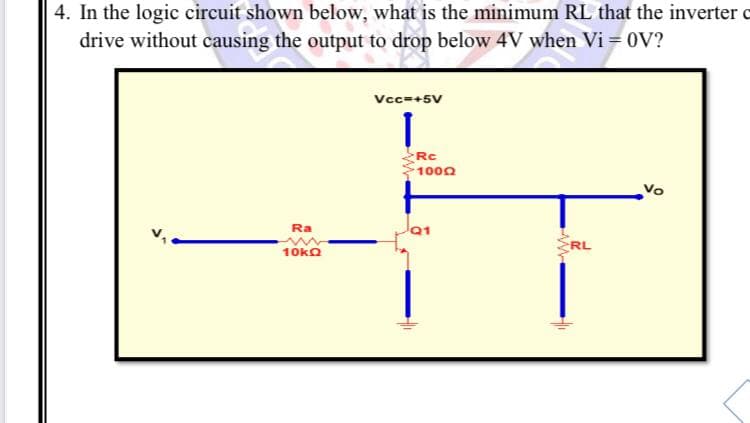
4. In the logic circuit shown below, what is the minimum RL that the inverter drive without causing the output to drop below 4V when Vi = 0V? Vcc=+5V Rc 1000 Vo Ra 10ko RL


Q: 3.(a) Make a truth table for this given logic gate, as shown in the figure. Show the steps. What is…
A: “Since you have asked multiple questions, we will solve the first question for you. If you want any…
Q: Design a counter that counts 1-2-3-5-7 Please explain the following:state diagram state table…
A:
Q: ülebäi The logic circuit represented by the figure shown below is A Doz B OR O AND O NAND O NOR O
A:
Q: You construct a gate level program using the provided circuit schematic. How many different logic…
A: The given circuit diagram is shown below,
Q: 3) Reduce (Simplify) the logic circuit expression A BU
A: Given logic circuit,
Q: Draw the logic diagram for the following functions, then map it using NAND only technology and NOR…
A:
Q: 4. In the logic circuit shown below, what is the minimum RL that the inverter can drive without…
A:
Q: A) Draw a logic circuit to realise the following expression using AND gates, OR gates and inverters.…
A:
Q: Draw full circuit
A: Diagram of ECL implementation
Q: We want to design a circuit to detect prime numbers. The input of the circuit is a 4-bit binary…
A:
Q: The logic swing in the inverter as shown is reducedby a factor of 3 by reducing the value of RCand…
A: Calculating collector resistance RC’ Calculating logic swing voltage
Q: Draw a logic diagram of a divide-by-14 counter using IC 7493 and 2-input AND gate.
A: We need to design a logic diagram of a divide-by-14 counter using IC 7493 and 2-input AND gate.…
Q: Prove (A+B)(A+C) = A+BC. Draw the logic circuit diagram for both sides
A:
Q: Assume that you need 0.6 V across RE to properlystabilize the current in the modified ECL gateas…
A: Given logic swing = 0.4 V, average current = 1 mA. Calculating voltage at low logic level…
Q: 2. Use two AND gates, two NOR gates and one INVERTER to construct the D latch circuit shown in…
A: It is D latch which is modification of SR lstch In SR latch at s=1,R=1 output state is invalid so…
Q: Q2. Minimize the combinational logic circuit in the following figure using Karnaugh's map only.…
A:
Q: Draw the logic circuit diagram using pure NAND gates and pure NOR gates: А В А ВСD Note: convert…
A: digital electronics problem.. Look below for the solution once...
Q: QUESTION 1 True or False (correct the sentence if false): 1. An inverter performs a NOT operation.…
A: We are authorized to answer three subparts at a time, since you have not mentioned which part you…
Q: Q2:Draw the logic circuit to Storage the data (110110).
A: As per the guideline we need to solve only first question. we need to draw the logic circuit to…
Q: Figure Q.4 (a) shows a combinational logic circuit with output, Z and Table Q.4(a) depicts the delay…
A: According to the question, for the figure shown below We need to find the critical path and…
Q: Consider a family of logic gates that operates under the static discipline with the following…
A: According to the question, we need to find noise margins The data are given as the following voltage…
Q: 3.36 Draw the logic diagram of the digital circuit specified by the following Verilog description:
A: In the given verilog code we have to draw the logic diagram of the verilog code
Q: Doe Do Dor Do Vị V3 Figure 2: Simulating delays with inverters. Let each inverter have delay A, then…
A: Given the logic circuit as shown below: We need to construct this circuit using the MUX circuit. We…
Q: Q.4 Draw the logic diagram to implement the following expression with minimum number of NAND gates.…
A: To implementation using NAND gate, the Boolean expression should be modified as- X=(A+B'+C')'…
Q: "For the logic circuit chown below FA F F=AB'+AB O E-A+B O F-AB F-A+B O
A: In this answer we will try to find the value of F as explained below.
Q: Q4: Given the table below that shows the tcp and tpp for each of the logic gate in the circuit…
A:
Q: Draw the logic circuit for (a'+ b'+ c + d) (a+ b+ c'+ d) (a+ b'+ c +d) using NOR gates.
A: The solution is as follows.
Q: Due to availability of NAND gate ICs only, design a digital logic circuit for the following…
A:
Q: Minimize the combinational logic circuit in the following figure using Karnaugh's map only.…
A: K-MAP: K-Map is used to optimize the Boolean function by using grouping technique. It's also being…
Q: In the logic circuit shown below, what is the minimum RL that the inverter can drive without causing…
A: Given Vi = 0 V V0 = 4 V Vcc = 5 V Rc = 100
Q: Draw a logic diagram using only two-input NAND gates to implement the following expression: F=(AB +…
A:
Q: 4. CMOS Logic Gate The PUN of a CMOS Logic Gate is shown below Vdd B-d 02 c 'Q3 B-das A-예- Q6 Q4 Q7…
A:
Q: Draw and explain the operation in detail (while including necessary table) the block diagram and…
A:
Q: The circuit on the right consists of an inverter connected to a load. Suppose that the range of…
A: According to the question, we need to determine the restriction for load resistance for the given…
Q: 2- In the logic circuit shown below, what is the minimum R, that the inverter can drive without…
A:
Q: How many 7400 ICs (minimum count) will be needed to execute the logic function F = A'B'C + AB'C' +…
A:
Q: Design a logic circuit to provide an odd parity bit for a 3-bit octal code. Draw the logic circuit…
A:
Q: Consider a dynamic domino logic circuit shown below. Suppose that each transistor has an internal…
A: Given : WN1 = WN2 = WN3 =1 u WP1 =2 u WP-1n =2u WN-1n=1 u L= 1 u Solution(a) The powee absorbed by…
Q: a) A standard TTL inverter gate is shown in the figure. The supply voltage is 5V. Calculate the…
A: Solution (a) - When Vi =0.1 V Thus, when the input voltage is 0.1 V than output voltage is 4.28 V.
Q: Design the logic circuit of a 3 to 8 line decoder with only NOR and NOTgates.
A:
Q: 29. The following figure shows the circuit design of logic operations. Select a FALSE statement.…
A: The given circuit design of logic operations is shown below,
Q: Using the DC operating conditions from the following table, give the noise margin LOW (NML) for the…
A: To find noise margin LOW(NML) for 74HC logic family with Vcc = +3.4v
Q: An equation in reduced SOP form is F=AB+B'C+A'C' I need to figure out how to draw a logic circuit…
A: we need to draw logic circuit for given function using NAND gates.
Q: Z= (A+B + CDE)+ B CD
A: The function is given as, Z=A+B+C-DE-+B-CD-
Q: 2. For the below logic circuit, draw the Waveforms at the numbered points. A A B B D D E E F F
A:
Q: 4) Design a saturated-load gate that implements the logic function Y = A(B +C D) + E . base on the…
A: Logic gates- Logic gates are mathematical exponential process deals with true or false values…

Step by step
Solved in 2 steps with 2 images

- Draw the schematic for a four-input NOR gate witha saturated load device. What are the W/L ratios ofall the transistors, based on the reference inverter ? (b) What is VL if all the logic inputs are equal to 1?F=A+B'C+A'BC' I need to construct the circuit in multism with an inverter, and gate, or gate.Simplify the expression G = (X’ + Y + Z’) (W + X + Y + Z) (W’ + X’ + Y’) using K- map and draw the corresponding simplified logic gate circuit.
- Q1: Design a combinational circuit with four inputs lines that represent a decimal digit in BCD and four output lines that generate the 9’s complement of the input digit. Q: 2 Show how a full adder can be converted to full-subtractor with the addition of one inverter circuit.From the equation A' B C' + A B C D, draw the combinational minimised logic circuit using respective Logic gate symbolsWhich of the following is an important feature of the sum-of-products form of expressions? • The delay times are greatly reduced over other forms. • The maximum number of gates that any signal must pass through is reduced by a factor of two. • No signal must pass through more than 2 gates (not including inverters). • All logic circuits are reduced to nothing more than simple AND and OR gates.
- Find VH , VL , and the power dissipation (forvO = VL ) for the logic inverter with resistor load. (b) Repeat for . P6.37(b)Provide the correct answer and write a legible solution. 1. Simplify the expression F = ABCD + AB’CD + A’B’C’D using Karnaugh map method and draw the corresponding simplified logic gate circuit.Convert the BCD to Excess-3 converter to its NOR gate equivalent form. Draw the logic diagram (Not the IC diagram) of the minimized NOR gate equivalent circuit (Give me the answer correctly and calculation also )
- How would you manipulate this equation to get it into a format where you can draw it as a NAND and inverter gates logic diagram and a NOR and inverter gates logic diagram?Design a 4-bit synchronous binary upcounter using T flip-flops. Draw only the logic diagram. Please show the process.Implement a 1-bit full adder circuit by using 4x1 MULTIPLEXER and an INVERTER. Data inputs are A, B, Cin and name the outputs as Sum, Cout.