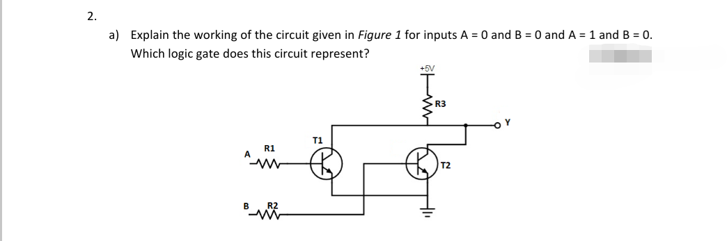
a) Explain the working of the circuit given in Figure 1 for inputs A = 0 and B = 0 and A = 1 and B = 0. %3D Which logic gate does this circuit represent?


Q: 2.3. (a) Differentiate comparatively the analogue and digital representations. (b) If 33210 = Xg…
A: Analog representations is the physical attributes without any difference between those which carry…
Q: For the logical gate shown in figure (4) if A is low (logic 0) and B (logic 0), then what is the…
A: Solution- Assume a single segment and analyze it, Given, A and B are at logic zero, So the…
Q: Draw full circuit
A: Diagram of ECL implementation
Q: 1. Code Conversion: Implement the logic circuit of a code converter that converts from the 8, 4,-2,…
A: Implement code converter from 8,4,-2,-1 to 8,4,2,1 code or BCD code ?
Q: Question 5. Consider the implementation of a logic function using a decoder given in figure 2 and…
A:
Q: Prove (A+B)(A+C) = A+BC. Draw the logic circuit diagram for both sides
A:
Q: 1. Explain how you can get a logical high output when using OR gate? 2. Explain how you can get a…
A: Disclaimer: Since you have asked multipart questions, we will solve the first three subpart for…
Q: Derive the state table and the state graph for the following logic circuit: A' B' B DA Clock Clock X…
A: The solution is given below
Q: Q2: Answer Two only: A) Simplify the circuit in Figure (1) as much as possible, and verify that the…
A: As per company guidelines we are supposed to answer only one question. Kindly repost other questions…
Q: Q1) Design a full Subtractor circuit that performs the subtraction of three bits: (A), (B) and (X),…
A:
Q: An engineer hands you a piece of paper with the following Boolean expression on it, and tells you to…
A: Given data, F = AB+ C(A+B).
Q: c) Explain the working of the circuit given in Figure 4 for inputs A =0 and B = 1. Give the value of…
A:
Q: 2. Realize the following function F(A_B.C.D) =E(1,2,5,6,7,11) using a (a) 4-to-1 multiplexer, and…
A:
Q: ii By analyzing the following two logic functions, identify the static hazards and draw the hazard…
A: In this question we have to find the static hazard
Q: Fill in the truth table below. Draw the Karnaugh map and show it in its simplest form. Draw the…
A:
Q: 2) For each of the following expressions, construct the corresponding logic circuit using only AND…
A: The solution can be achieved as follows.
Q: State in detail the reason why logic circuits are minimized
A: Advantages of minimization of logic gates?
Q: Part B : Answer all questions in the space provided with working steps. 1. Draw the logic circuit…
A: So we can use maximum 5 nand gate.
Q: F a) Write the switching expression for the output, F(A,B,C,D) b) Simplify this switching function…
A: To simplify output, we will follow outputs from each gates and so on we can conclude final output F.…
Q: A logic function f(A,B,C) implemented with 4x1 MUX circuit. Implement the same function with using…
A:
Q: 2. Consider the following operation: Z = AB BC a. Write out the truth table for the given…
A: Given operation Z = AB.BC The truth table, logic circuit and the implementation…
Q: A В C
A:
Q: 2. Consider the following operation: Z = AB BC a. Write out the truth table for the given…
A: Given,The boolean opeartion is,Z=AB·BC
Q: Q2: Draw a Flowchart to perform the function (G) for the logic circuit shown below, that outputs are…
A: Given
Q: A B ·Y
A:
Q: Create a logic diagram out of this boolean expression. CD+BD+BC+AD+AC+AB Note: All inputs A B C…
A: Please find the attachment
Q: c) Explain the working of the circuit given in Figure 4 for inputs A = 0 and B = 1. Give the value o…
A: Brief description : Here diodes are used to justify the logic gate of the given circuit. According…
Q: Figure 3 Figure 1 21 21 DE Figure 4 Figure 2 21 Figure 5 JSE THE TRUTH TABLE TO JUSTIFY THE LOGIC…
A: Given With the help of truth table for all the given figures we calculated the output equation…
Q: 17. Draw the logic circuit represented by each of the following expressions: (b) (A+B)(C+D+E) (a)…
A: We are authorized to answer one question at a time, since you have not mentioned which question you…
Q: (b) Analyse the sequential logic circuit for the D Flip-Flop shown in Figure below and answer the…
A: (i) The flip flop input and output equations are given by: DA = XA + XB DB = A'X Z = X' (A+B) In…
Q: Answer the following questions: i. If a 3-input XOR gate has eight input possibilities, how many of…
A: (i) 3 input X-OR gate symbol present as, Where output, w=x⊕y⊕z
Q: 16) Answer each of the following with reference to the overfill alarm program shown in the figure…
A: “Since you have posted a question with multiple sub-parts, we will solve the first three sub-parts…
Q: Draw and explain the operation in detail (while including necessary table) the block diagram and…
A:
Q: Find a logic diagram that corresponds to the VHDL structural description in below figure. Note that…
A: In the structural model, the hardware is described as the interconnection of modules. Any instance…
Q: A coin-operated cold drink dispenser will provide cold drink (D) under the following conditions:…
A: The solution can be achieved as follows.
Q: A logic program produces set of logic data as depicted in the Table 2 below. This logic program…
A:
Q: 3.5 Design a logic circuit from the following switch function using Boolean theory using only NOR…
A:
Q: Q3) a- Draw the logic diagram for a circuit that will divide the (fcLK) by 32. Use (+ve) edge…
A:
Q: 2. Simplify the logic function f = A+ BC + A(B + C) and draw a schematic for the circuit that…
A: The digital circuits can be combinational as well as sequential circuits. The combinational circuits…
Q: 1. Design a simple logic circuit for a Set/Reset (SR) Latch, based on any actual application of…
A:
Q: Draw the F1 and F2 outputs of the above logic circuit only with OR NOT gates and A, B, C, D…
A:
Q: D- A в H Figure 1 3. Referring to the logic circuit in Figure 1, determine: a. The simplified…
A:
Q: Given the logic function: F(A,B,C,D) = Σm(0,4,5,10,11,13,14,15) a. Find a minimum circuit which…
A: It is given that: F(A,B,C,D) = Σm(0,4,5,10,11,13,14,15)
Q: a) Explain the working of the circuit given in Figure 1 for inputs A = 0 and B = 0 and A = 1 and B =…
A: the circuit is given as
Q: Q3) a- Draw the logic diagram for a circuit that will divide the (fcLK) by 16. Use (-ve) edge…
A: The digital circuits can be combinational as well as sequential circuits. The combinational circuits…
Q: Below is an NMOS logic circuit. For all of the MOSFETs assume V = 1 V and k = 50 mA/V². th 5V 5V R₂…
A: Given question is related to logic family circuits
Q: 4x1 MUX La 1,
A:
Q: 14. Identify each logic gate shown on the given diagrams A D
A: Logic gate AND , OR , NAND, NOT, NOR GATE?
Q: [Part.2] Manually draw the logic diagram of 4x1 Multiplexer below (with depicting the internal…
A: Multiplexer- It is a combinational circuit that selects several inputs and forwards them to a single…

Step by step
Solved in 3 steps with 1 images


- (a) Differentiate comparatively the analogue and digital representations. (b) If 33210= Xs then find the value of X. (c)1001011.0112 to equivalent decimal (d) What do you know about the logic gates? Explain the AND gate in details. 410 A1) Design the logic gates that compare (3) bit binary numbers that are "equal" or "not equal." A0 B0 A1 B1 A2 B2 2) Derive the logic equations for both outputs 3) What type of circuit/system can this be used in an application you could create?Binary Subtractors 1. What are binary subtractors? 2. How does it work? 3. Types of binary subtractors. 4. Draw the logic circuit diagram. 5. Show the truth table. (Our subject is logic circuit and switching theory, and our lesson is combination logic circuit)
- Book used is Digital Logic with Verilog Design by Brown & Vranesic. Study the counting circuit diagram below and answer the following questions: a. Based on the circuit drawing, is the Clock Positive-Edge Triggered or Negative-Edge Triggered? b. How was this determination made? c. What are the minimum and maximum valkues of the circuit? Explain. d. There are 3 grayed out boxes we refer to this symbolic use as _____________. Why are these used in circuit design?Given the logic function: F(A,B,C,D) = Σm(0,4,5,10,11,13,14,15) a. Find a minimum circuit which implements F using AND and OR gates. Identify two 1-hazards in the circuit. b. find another minimum circuit which implements F using AND and OR gates. Identify two 0-hazards in the circuit. c. Find an AND-OR circuit for F which has no hazards.There are 5 gates in a metrobus, 1 of which is to get on and 4 to get off. The number of passengers inside is desired to be seen on the LCD connected to the P2 port. Get-on gate is controlled by the P0.2 while get-off gates are controlled by the P0.3, P0.4, P0.5, and P0.6. The sensors generate Logic-1 while passing passengers. Since the passenger carrying capacity of the metrobus is 294, if the number of passengers exceeds the number of 294, the warning LED connected to the P0.7 pin is required to light up. Since other pins of P0 are used for other purposes, it is not desired to be changed. Can you write the answer with assembly code using 8051 - AT89S8253 architecture?
- choose the correct answer If a two-input logic gate produces a output of logic HIGH, only if both inputs are different, then the logic gate is? a. IC 7400 b. IC 7486 c. IC 7408 d. IC 7432Create the logic diagram of the two bits full adderWe want to design a circuit to detect prime numbers.The input of the circuit is a 4-bit binary number and the output is a single bit and should show one when the number is prime and zero otherwise.B. Implement the circuit using a 4× 1 multiplexer and combinational logic gates.C. Implement the circuit using only one decoder and one OR gate. What is the size of the decoder you use?