Assume that the microprocessor can directly address 64K with a and 16 data pins The memory map for 16K x 16 RAM system that design by using 8KX8 RAM are None of them C000-DFFF, A000-BFFF, 8000-9FFF, 6000- ZEFF 0000-1FFF , 2000-3FFF, 4000-5FFF, 6000- ZEFF 1000-1FFF, 2000-2FFF, 4000-4FFF, 8000-8FFF E000-EFFF, D000-DFFF, B000-BFFF, 7000- ZEFF
Assume that the microprocessor can directly address 64K with a and 16 data pins The memory map for 16K x 16 RAM system that design by using 8KX8 RAM are None of them C000-DFFF, A000-BFFF, 8000-9FFF, 6000- ZEFF 0000-1FFF , 2000-3FFF, 4000-5FFF, 6000- ZEFF 1000-1FFF, 2000-2FFF, 4000-4FFF, 8000-8FFF E000-EFFF, D000-DFFF, B000-BFFF, 7000- ZEFF

Chapter4: Processor Technology And Architecture
Section: Chapter Questions
Problem 2PE: If a microprocessor has a cycle time of 0.5 nanoseconds, what’s the processor clock rate? If the...

Related questions
Topic Video
Question
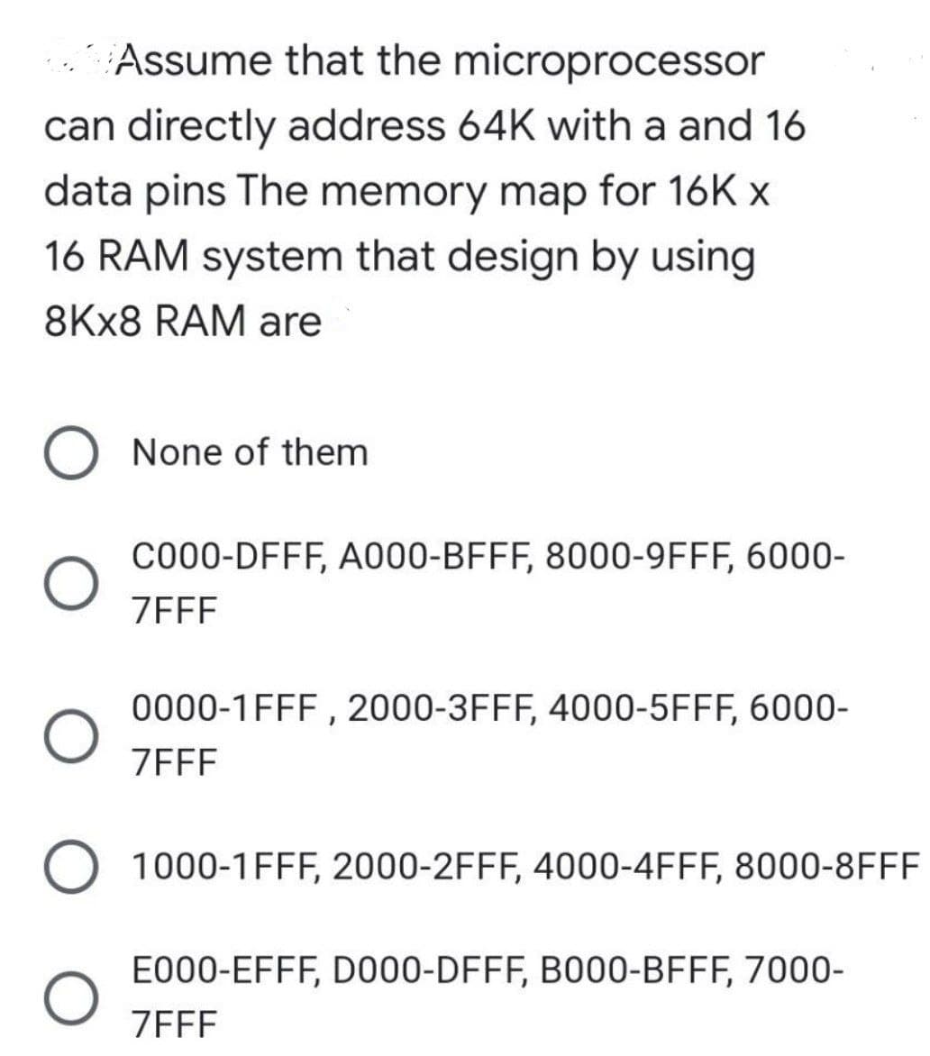
Transcribed Image Text:Assume that the microprocessor
can directly address 64K with a and 16
data pins The memory map for 16K x
16 RAM system that design by using
8KX8 RAM are
O None of them
C000-DFFF, A000-BFFF, 8000-9FFF, 6000-
ZEFF
0000-1FFF , 2000-3FFF, 4000-5FFF, 6000-
ZEFF
1000-1FFF, 2000-2FFF, 4000-4FFF, 8000-8FFF
E000-EFFF, D000-DFFF, B000-BFFF, 7000-
ZEFF
Expert Solution
This question has been solved!
Explore an expertly crafted, step-by-step solution for a thorough understanding of key concepts.

This is a popular solution!

Trending now
This is a popular solution!

Step by step
Solved in 2 steps

Knowledge Booster


Learn more about
Need a deep-dive on the concept behind this application? Look no further. Learn more about this topic, computer-science and related others by exploring similar questions and additional content below.Recommended textbooks for you
Systems Architecture
Computer Science
ISBN:
9781305080195
Author:
Stephen D. Burd
Publisher:
Cengage Learning
Fundamentals of Information Systems
Computer Science
ISBN:
9781305082168
Author:
Ralph Stair, George Reynolds
Publisher:
Cengage Learning
Systems Architecture
Computer Science
ISBN:
9781305080195
Author:
Stephen D. Burd
Publisher:
Cengage Learning
Fundamentals of Information Systems
Computer Science
ISBN:
9781305082168
Author:
Ralph Stair, George Reynolds
Publisher:
Cengage Learning