(b) Write the Boolean Expression from the given logic circuit in Figure Q5 (B). AD B DC Figure Q5 (B)
(b) Write the Boolean Expression from the given logic circuit in Figure Q5 (B). AD B DC Figure Q5 (B)

Chapter22: Sequence Control
Section: Chapter Questions
Problem 6SQ: Draw a symbol for a solid-state logic element AND.

Related questions
Question
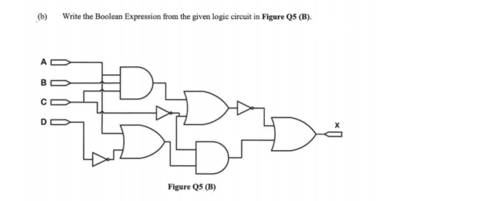
Transcribed Image Text:(b)
Write the Boolean Expression from the given logic circuit in Figure Q5 (B).
A C
BO
D
Figure Q5 (B)
Expert Solution
This question has been solved!
Explore an expertly crafted, step-by-step solution for a thorough understanding of key concepts.

Step by step
Solved in 2 steps with 1 images

Knowledge Booster


Learn more about
Need a deep-dive on the concept behind this application? Look no further. Learn more about this topic, electrical-engineering and related others by exploring similar questions and additional content below.Recommended textbooks for you