) Design a single-digit decade counter that counts from 0 to 9 and repeats. The single-digit decade counter should be built by a cascaded synchronous binary counter (74LS163) and other basic logic gates. Simulate the complete counter circuit by OrCAD and PSPICE. Capture the circuit schematic and the simulated waveform. (Define the simulation timings for at least one full counting cycle from 0 to 9 and back to 0.) (Hint: Use the DigClock input from the SOURCE as shown below and setup the CLK ONTIME and OFFTIME accordingly for the clock source.)
) Design a single-digit decade counter that counts from 0 to 9 and repeats. The single-digit decade counter should be built by a cascaded synchronous binary counter (74LS163) and other basic logic gates. Simulate the complete counter circuit by OrCAD and PSPICE. Capture the circuit schematic and the simulated waveform. (Define the simulation timings for at least one full counting cycle from 0 to 9 and back to 0.) (Hint: Use the DigClock input from the SOURCE as shown below and setup the CLK ONTIME and OFFTIME accordingly for the clock source.)

Database System Concepts
7th Edition
ISBN:9780078022159
Author:Abraham Silberschatz Professor, Henry F. Korth, S. Sudarshan
Publisher:Abraham Silberschatz Professor, Henry F. Korth, S. Sudarshan
Chapter1: Introduction
Section: Chapter Questions
Problem 1PE

Related questions
Question
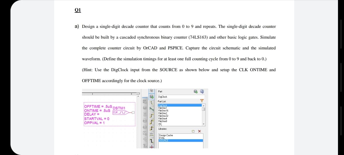
Transcribed Image Text:Q1
a) Design a single-digit decade counter that counts from 0 to 9 and repeats. The single-digit decade counter
should be built by a cascaded synchronous binary counter (74LS163) and other basic logic gates. Simulate
the complete counter circuit by OrCAD and PSPICE. Capture the circuit schematic and the simulated
waveform. (Define the simulation timings for at least one full counting cycle from 0 to 9 and back to 0.)
(Hint: Use the DigClock input from the SOURCE as shown below and setup the CLK ONTIME and
OFFTIME accordingly for the clock source.)
Part
DigClock
Part List:
OFFTIME = .5uS DSTM1
ONTIME = .5us
DELAY =
STARTVAL = 0
OPPVAL = 1
DisClock
FileStm1
FieStm16
CLK
FileStim2
FileStim32
FileStim4
FileStime
Libraries
Design Cache
EVAL
1.
SOURCE
Expert Solution
This question has been solved!
Explore an expertly crafted, step-by-step solution for a thorough understanding of key concepts.

This is a popular solution!

Trending now
This is a popular solution!

Step by step
Solved in 2 steps with 1 images

Knowledge Booster


Learn more about
Need a deep-dive on the concept behind this application? Look no further. Learn more about this topic, computer-science and related others by exploring similar questions and additional content below.Recommended textbooks for you
Database System Concepts
Computer Science
ISBN:
9780078022159
Author:
Abraham Silberschatz Professor, Henry F. Korth, S. Sudarshan
Publisher:
McGraw-Hill Education

Starting Out with Python (4th Edition)
Computer Science
ISBN:
9780134444321
Author:
Tony Gaddis
Publisher:
PEARSON

Digital Fundamentals (11th Edition)
Computer Science
ISBN:
9780132737968
Author:
Thomas L. Floyd
Publisher:
PEARSON
Database System Concepts
Computer Science
ISBN:
9780078022159
Author:
Abraham Silberschatz Professor, Henry F. Korth, S. Sudarshan
Publisher:
McGraw-Hill Education
Starting Out with Python (4th Edition)
Computer Science
ISBN:
9780134444321
Author:
Tony Gaddis
Publisher:
PEARSON
Digital Fundamentals (11th Edition)
Computer Science
ISBN:
9780132737968
Author:
Thomas L. Floyd
Publisher:
PEARSON

C How to Program (8th Edition)
Computer Science
ISBN:
9780133976892
Author:
Paul J. Deitel, Harvey Deitel
Publisher:
PEARSON

Database Systems: Design, Implementation, & Manag…
Computer Science
ISBN:
9781337627900
Author:
Carlos Coronel, Steven Morris
Publisher:
Cengage Learning

Programmable Logic Controllers
Computer Science
ISBN:
9780073373843
Author:
Frank D. Petruzella
Publisher:
McGraw-Hill Education