(ii) What is the origin of the positively charged holes in the valence band ? Are these positive charges mobile or stationary when we apply an electric field ? Answer: (iii) What is the origin of the negatively charged electrons in the conduction band ? Are these negatively charged electrons mobile or stationary when we apply an electric field ? 9. Answer:
(ii) What is the origin of the positively charged holes in the valence band ? Are these positive charges mobile or stationary when we apply an electric field ? Answer: (iii) What is the origin of the negatively charged electrons in the conduction band ? Are these negatively charged electrons mobile or stationary when we apply an electric field ? 9. Answer:

Power System Analysis and Design (MindTap Course List)
6th Edition
ISBN:9781305632134
Author:J. Duncan Glover, Thomas Overbye, Mulukutla S. Sarma
Publisher:J. Duncan Glover, Thomas Overbye, Mulukutla S. Sarma
Chapter4: Transmission Line Parameters
Section: Chapter Questions
Problem 4.2P: The temperature dependence of resistance is also quantified by the relation R2=R1[ 1+(T2T1) ] where...

Related questions

Question
question in photo plz
Transcribed Image Text:(ii) What is the origin of the positively charged holes in the valence band ? Are these positive charges
mobile or stationary when we apply an electric field ?
Answer:
(iii) What is the origin of the negatively charged electrons in the conduction band ? Are these
negatively charged electrons mobile or stationary when we apply an electric field ?
Answer:
(iv) What is the relative energies (order of magnitude) for the values of E and EA ?
Answer:
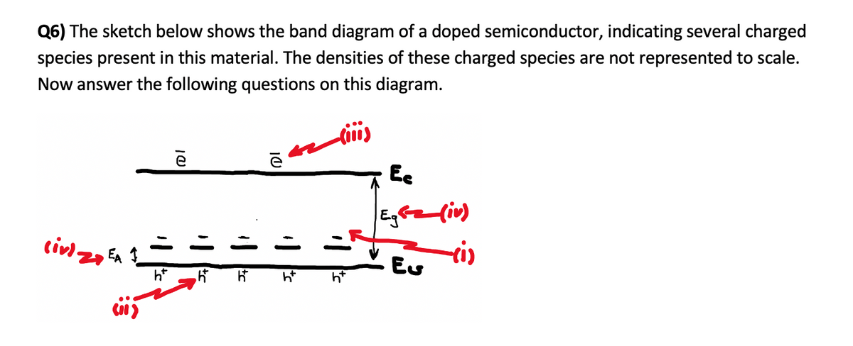
Transcribed Image Text:Q6) The sketch below shows the band diagram of a doped semiconductor, indicating several charged
species present in this material. The densities of these charged species are not represented to scale.
Now answer the following questions on this diagram.
e
Ee
Egfe (iv)
Eu
h*
ht
ht
10
Expert Solution
This question has been solved!
Explore an expertly crafted, step-by-step solution for a thorough understanding of key concepts.

Step by step
Solved in 3 steps

Knowledge Booster


Learn more about
Need a deep-dive on the concept behind this application? Look no further. Learn more about this topic, electrical-engineering and related others by exploring similar questions and additional content below.Recommended textbooks for you
Power System Analysis and Design (MindTap Course …
Electrical Engineering
ISBN:
9781305632134
Author:
J. Duncan Glover, Thomas Overbye, Mulukutla S. Sarma
Publisher:
Cengage Learning

Delmar's Standard Textbook Of Electricity
Electrical Engineering
ISBN:
9781337900348
Author:
Stephen L. Herman
Publisher:
Cengage Learning
Power System Analysis and Design (MindTap Course …
Electrical Engineering
ISBN:
9781305632134
Author:
J. Duncan Glover, Thomas Overbye, Mulukutla S. Sarma
Publisher:
Cengage Learning
Delmar's Standard Textbook Of Electricity
Electrical Engineering
ISBN:
9781337900348
Author:
Stephen L. Herman
Publisher:
Cengage Learning