---JIEN a 8x1 IM :* sino enable Di- line at hinh - ---. o cetive? 3- Design logic circuit by using a decoder which represents the equation F(A,B)-Σ(0, 1,2)? 4- Design full adder by using a decoder? %3D
---JIEN a 8x1 IM :* sino enable Di- line at hinh - ---. o cetive? 3- Design logic circuit by using a decoder which represents the equation F(A,B)-Σ(0, 1,2)? 4- Design full adder by using a decoder? %3D

Chapter22: Sequence Control
Section: Chapter Questions
Problem 6SQ: Draw a symbol for a solid-state logic element AND.

Related questions
Question
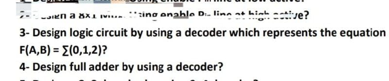
Transcribed Image Text:--JIEN a 8x1 v : sing enable Di- line at hinh -
---. o
cetive?
3- Design logic circuit by using a decoder which represents the equation
FA,B)-Σ(0, 1,2)?
%3D
4- Design full adder by using a decoder?
Expert Solution
This question has been solved!
Explore an expertly crafted, step-by-step solution for a thorough understanding of key concepts.

Step by step
Solved in 3 steps with 3 images

Knowledge Booster


Learn more about
Need a deep-dive on the concept behind this application? Look no further. Learn more about this topic, electrical-engineering and related others by exploring similar questions and additional content below.Recommended textbooks for you