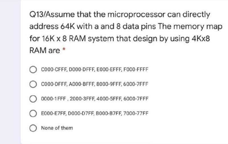
13/Assume that the microprocessor can directly address 64K with a and 8 data pins The memory m or 16K x 8 RAM system that design by using 4KX8


Q: Assume two secondary memory processes exist. In light of phase 1, one priority is higher than the…
A:
Q: Q8/Assume that the microprocessor can directly address 64K with a R/W' and 8 data pins The memory…
A: option b
Q: The CPU we are talking about today is intel core i7- 8750H 64 bit write in detail about the below…
A: The i7-8750H functions at 2.2 GHz with a TDP of 45 W and a turbo boost of up to 4.1 GHz. This chip…
Q: Q3/Assume that the microprocessor can directly address 64K with a 16 data pins The memory map for…
A: The question is to choose the correct option for the given question.
Q: Back in the days, main memory modules used to be quite small in size. One such a module was of size…
A: Byte addressable memory name itself states that it requires 1 byte (8 bits) of space for storing…
Q: MOV R2, [R5]: here [R5] refers memory locations and R5 contains memory address SUB R5, RI, R4; a)…
A: In questions with multiple questions, we must solve only the first one.
Q: 3- The 8086 Processor has several control lines, in considering that. Explain the following: a.…
A: Main points about : It is 16 bit , N channel , HMOS(High Speed Metal Oxide) processor.It is 40 pin…
Q: In the MC68000 microprocessor, the total memory address is 16 MB and it is based on address pins. i.…
A: Answer: I have given answer in the brief explanation.
Q: Q13/Assume that the microprocessor can directly address 64K with a and 8 data pins The memory map…
A: asssume that the microprocessor can directly address 64k with a and 8 data pins the memory map for…
Q: 1. What is the main disadvantage & advantage of the stack as temporary storage compared to having a…
A: Introduction: A stack storage structure follows the last in first out method while storing and…
Q: We know that CPU may cache memory access. Should we allow memory-mapped device I/O to be cached by…
A:
Q: 9- Design a simple memory of type RAM starting from address 0001 to 0110 with memory width is 8…
A: Actually, memory is used to stores the data.
Q: 1 a) Differentiate between Intel 8085 microprocessor and Intel 8086 microprocessor b) The 8085…
A: To answer the following question: a. Differentiate between Intel 8085 and 8086 micropocessor b. Name…
Q: Assume that the Multi-Cycle CPU discussed in the class is updated to support various new RSIC-V…
A: Answer: Given ROM 212 X17 212 X 25 =217 (Because 17 beyond 24 and before 25)
Q: Hand draw a microprocessor with all the essential components, busses alu, microarchitecture,cache,…
A:
Q: A memory unit has a capacity of 65,536 words of 25 bits each. It is used in conjunction with a…
A: *As per the company norms and guidelines we are providing a first question answer only please repost…
Q: Q8/Assume that the microprocessor can directly address 64K with a R/W and 8 data pins The memory map…
A: Given:
Q: Q13/Assume that the microprocessor can directly address 64K with a and 8 data pins The memory map…
A: Assume that the microprocessor can directly address 64k with a and 8 data pins the memory map for…
Q: Q13/Assume that the microprocessor can directly address 64K with a and 8 data pins The memory map…
A: check further steps for the answer :
Q: Answer the following short questions. Support your answers with diagram, where needed: How the LIFO…
A: Lets see the solution.
Q: 3) Assume a 232 byte memory system a) What are the lowest and highest addresses if memory is byte…
A: Given: 232 byte memory system, we have find the solution for the following What are the lowest and…
Q: 12-5. A computer employs RAM chips of 256 × 8 and ROM chips of 1024 × 8. The computer system needs…
A: In this question we have given some information related to size of memory components and we need to…
Q: Memory address translation is useful only if the total size of virtual memory (summed over all…
A: Virtual memory address translation is useful even if the total size of the virtual memory (summed…
Q: The lastest data access is provideu DRAM's. A B SRAM's. C Registers. Caches. D
A: Please find the answer below
Q: Instructions Space MAR ALU MBR AC BUS PC Control Data Space Cache A simple processor shown in the…
A: subtraction, addition and multiplication operations are given below:- by bartleby guidelines i am…
Q: f the processor has 31 instructions and a 64MB memory and each data is 2 bytes wide, what is the…
A: The correct in questions Option is("c")"54"
Q: b. separate memories. c. either in the same memory or in a separate memories. 2. Processing speed of…
A: Answer :Following are the answers for the above fill in blanks: 1. In Von Neumann architecture…
Q: Q8/Assume that the microprocessor can directly address 64K with a R/W' and 8 data pins The memory…
A: Please check the solution below
Q: 4. a) A 4Kb (kilobyte) RAM chip is required in a microprocessor system with a 12-bit address bus and…
A: Solution:-- 1)The given question has required for the solution to be provided with an answer…
Q: You are participating in a Hackathon and you have been assigned a task to add a module to a newly…
A: Below is the properly step by step well explained code. Let’s identify variables needed for this…
Q: Q12/Assume that the microprocessor can directly address 1M with a and 8 data pins, The maximum RAM…
A: I have answered this question in step 2.
Q: Microprocessor Systems Question: Intel's AURORA processor can access up to 10 PB of byte indexed…
A: Aurora is a planned supercomputer to be completed in 2021. It will be the United States' second…
Q: 1. Briefly explain the following terms used for Intel 8086 microprocessor with appropriate…
A: PUSH : This instruction works with 16 bit values only and used for STACK INSERTION Used to store…
Q: 27. A memory connected to microprocessor has 20 addı 16 data lines. What will be t canacit?
A: It will have a memory capacity of 2MB
Q: Given a 32M x 16 bit memory chip. Answer the following questions. a) Draw the memory chip. Label…
A:
Q: 27. A memory connected to a microprocessor has 20 address lines and 16 data lines. What will be the…
A: INTRODUCTION: Here we need to calculate the total memory capacity.
Q: /Assume that the microprocessor can directly address 64K with a R/W' and 8 data pins The memory map…
A: Given that, a microprocessor can directly address 64K with a R/W and 8 data pins. That means it…
Q: CLO2.2: A memory unit consists of 8k words with each word consisting of 16 bits. How many address…
A: The answer is Option A.
Q: CPU Main Memory Instructions Space MAR ALU MBR AC BUS PC Control Data Space Cache A simple processor…
A: Given is in a reaction between Fe+3 and NCS-, Kc = 620.4 Volume of Fe+3 = 10 mL molarity of Fe+3 =…
Q: Q12/Assume that the microprocessor can directly address 1M with a and 8 data pins, The maximum RAM…
A: assume microprocessor can directly address 1M with a and 8 data pins , the maximum RAM systems can…
Q: 11. Which of the following is not a form of memory ? a. Instruction cache b. Instruction register c.…
A: c) Instruction opcode
Q: 4 Assuming the following integers in memory: 3000 2000 1000 1000 100 10 And the following integers…
A: About leal instruction:
Q: 27. A memory connected to a microprocessor has 20 address lines and 16 data lines. What will be the…
A: Let's see the solution that what will be the memory capacity
Q: IV.Consider a 32bit microprocessor which has an on chip 1Mbytes four-way set- associative cache.…
A:
Q: CPU Main Memory Instructions Space MAR ALU MBR AC BUS PC Control Data Space Cache A simple processor…
A: According to the guidelines i can answer only first 3 subparts
Q: PROBLEM STATEMENT- WRITE/STORE 10 NUMBERS IN THE MEMORY STARTING FROM ANY 16 BIT ADDRESS (E.G 2000…
A:
Q: Assume that the microprocessor can directly address 64K with a and 16 data pins The memory map for…
A: Step 1 The answer is given in the below step
Q: Answer the following question: 1-What is the datapath? 2-What is the Instruction cycle? 3-What is…
A: Answer the following question:1-What is the datapath?2-What is the Instruction cycle?3-What is the…
Q: Assume that one 32-bit and two 16-bit microprocessors are to be interfaced to a system bus. The…
A: The answer given as below:
Q: 8. A computer architect is designing the memory system for the next version of a processor. If the…
A: Part A 1.71 Part B Speedup = 5.99 Explanation: Fractionunused = 0.6…
Q: Q8/Assume that the microprocessor can directly address 64K with a R/W' and 8 data pins The memory…
A: Given: Assume that themicroprocessor can directlyaddress 64K with a R/W' and 8 data pins The memory…
Q: We want to build a word organized main memory of 8 GB for a 32-bit CPU architecture composed of word…
A: Solution:: Let's see the direct answer for the above question first then will see the basic part…


Step by step
Solved in 2 steps with 1 images


- Assume that the microprocessor can directly address 1M with a and 8 data pins. The maximum RAM system can design by using the following RAM chips is. Size of RAM chip Number of Chips 2K × 4 6 4K × 4 7 1k × 4 512 × 8 5 10 a. 27k × 8 b. 26k × 8 c. None of them d. 24k × 8 e. 25k × 82. This question is about Digital Logic and Address DecodingA computer is being designed using a microprocessor with a 16-bit address bus (A0—A15, where A0 is the least significant bit). The 64K address space is to be split betweenand allocated to RAM, ROM and I/O hardware as follows:Address Range (hex) Contains Select Signal0x0000 — 0x1FFF Main RAM RAMCS0x8000 — 0x9FFF Video RAM VRAMCS0xB000 — 0xBFFF I/O hardware IOCS0xC000 — 0xCFFF BASIC ROM BROMCS0xF000 — 0xFFFF OS ROM OSROMCSThe rest of the address space is unused.Note: As with many computer systems, it its only necessary to decode addresses to sufficiently identify each of the sections above uniquely. It is acceptable for some parts to be decodeable by more than one address provided these extra addresses do not overlap any of the other specified address ranges. Using a combination of AND, OR and NOT gates and the signals (A12 — A15) that contain the top four bits of the address in binary form: a. Derive the equation for a logic…We want to build a byte organized main memory of 8 GB for a 32-bit CPU architecture composed ofbyte organized memory modules of 30-bit address and 8-bit data buses each.a) Draw the interface of the main memory by clearly indicating the widths of the buses.b) How many memory modules would be necessary to build the memory system?c) Design the main memory internal organization built out of the above memory modules (usemultiplexers and/or decoders as needed) by clearly indicating the widths of the used bussesd) Can we use this memory system as RAM for the CPU in Problem 1? Explain your answer.
- 1) For a Pentium II descriptor that contains a base address of 0004B100H, a limit of 00FFFH, and G = 1, what starting and ending locations are addressed by this descriptor? 2) Code a descriptor that describes a memory segment that begins at location 0005CF00h and ends at location 00060EFFh. The memory segment is a data segment that grows upward in the memory system and can be written. The segment has a user level privilege (lowest) and has not been accessed. The descriptor is for an 80386 microprocessor.A computer is using a fully associative cache and has 216 bytes of main memory (byte addressable) and a cache of 64 blocks, where each block contains 32 bytes. a. How many blocks of main memory are there? b. What will be the sizes of the tag, index, and byte offset fields? c. To which cache set will the memory address 0xF8C9(hexadecimal) map?Suppose that a 2M × 16 main memory is built using 256K × 8 RAM chips and that memory is word addressable.1. a) How many RAM chips are necessary?2. b) If we were accessing one full word, how many chips would be involved? 3. c) How many address bits are needed for each RAM chip?4. d) How many banks will this memory have?5. e) How many address bits are needed for all memory?6. f) If high-order interleaving is used, where would address 14 (which is E in hex) be located?7. g) Repeat exercise 9f for low-order interleaving.
- Suppose that 16M × 16 memory built using 512K × 8 RAM chips and that memory is word addressable.1. a) How many RAM chips are necessary?2. b) If we were accessing one full word, how many chips would be involved? 3. c) How many address bits are needed for each RAM chip?4. d) How many banks will this memory have?5. e) How many address bits are needed for all memory?6. f) If high-order interleaving is used, where would address 14 (which is E in hex) be located?7. g) Repeat exercise 9f for low-order interleaving.Suppose that a 64M x 16 main memory is built using 512K × 8 RAM chips and memory is word-addressable. a) How many RAM chips are necessary?b) If we were accessing one full word, how many chips would be involved?c) How many address bits are needed for each RAM chip?d) How many banks will this memory have?e) How many address bits are needed for all of memory?f) If high-order interleaving is used, where would address 32(base 10) be located? (Your answer should be "Bank#, Offset#")g) Repeat (f) for low-order interleaving.We want to build a word organized main memory of 8 GB for a 32-bit CPU architecture composed of word organized memory modules of 30-bit address and 8-bit data buses each. a) Draw the interface of the main memory by clearly indicating the widths of the buses. b) Howmanymemorymoduleswouldbenecessarytobuildthememorysystem? c) Design the main memory internal organization built out of the above memory modules (use multiplexers and/or decoders as needed) by clearly indicating the widths of the used busses d) CanweusethismemorysystemasRAMfortheCPUinProblem1?Explainyouranswer.
- A microprocessor has an increment memory direct instruction, which adds 1 to the value in a memory location. The instruction has five stages: fetch opcode(four bus clock cycles),fetch operand address (three cycles), fetch operand (three cycles) add 1 to operand (three cycles), and store operand (three cycles). a. By what amount (in percent) will the duration of the instruction increase if we have to insert two bus wait states in each memory read and memory write operation? b. repeat assuming that the increment operation takes 13 cycles instead of 3 cyclesa) A block-set associative cache memory consists of 128 blocks divided into four block sets. The main memory consists of 32,768 blocks and each block contains 512 eight-bit words (1) How many bits are required for addressing the main memory? (ii) How many bits are needed to represent the TAG SET and WORD fields? b) Write a program to code the equation X=(A+B)L| ((C+D) using one-address instructions. Please solve only the b partQ 1. Answer the following short questions. Support your answers with diagram, where needed: How the LIFO memory differs to FIFO Memory. Which type of addressing mode is used by the Instruction: ADD [BX+2], AX? What is the equivalent of a Binary number: 00110100011012 in octal and hexa-decimal. How much memory space is addressable (in bytes) by a microprocessor, if it uses 36 address lines? If Base address = A000H, Physical address = A0345H, then the offset add = ___________? Why address bus is unidirectional and data bus is bidirectional in 8086?