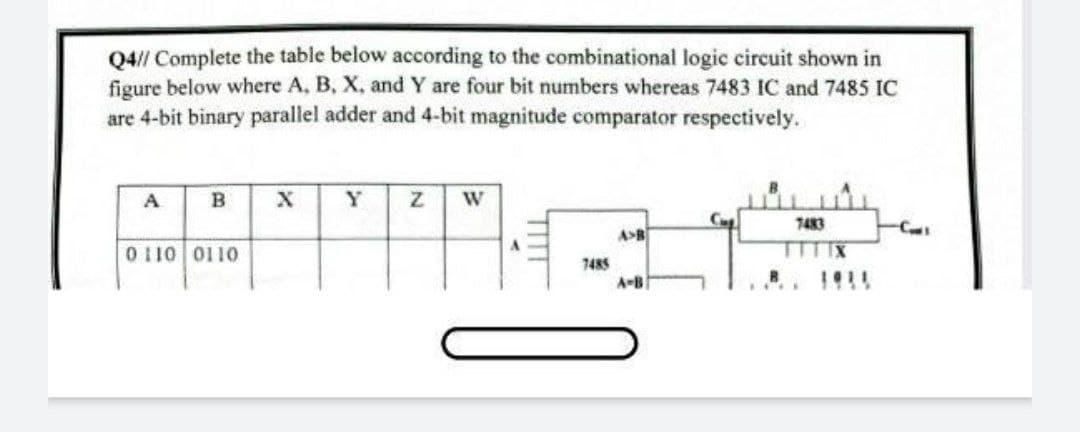
Q4// Complete the table below according to the combinational logic circuit shown in figure below where A, B, X, and Y are four bit numbers whereas 7483 IC and 7485 IC are 4-bit binary parallel adder and 4-bit magnitude comparator respectively. A B XYZ 7483 A>B 0 110 0110 TTTTX 7485 A-B


Q: Design a combinational logic circuit that takes a 3–bit input and has one output P. The P output…
A:
Q: 2.1 Design a magnitude comparator, that is able to detect whether A > B, A = B, A В, А 3 В, А B A =…
A: 2.1
Q: Design a sequential circuit that outputs 2’s complement of a bit sequence. The bit sequence will be…
A:
Q: 213. a) Draw the circuit generated by the following VHDL coc entity example is port(A, B: in bit;…
A:
Q: Explain a 4-bit arithmetic circuit alongwith its function table. Answer must include diagram of…
A: SUMMARY: - Hence, We discussed all the points.
Q: . Design a 16*1 MUX using 4 *1 MUXs.
A: Actually, given question regarding multiplexers.
Q: 1- Perform a comparison of the combinational circuit and the sequential circuit that realize the add…
A: Answer is given below-
Q: Design an unsigned 8-bit divide-by-ten circuit which gives the output as Quotient and Remainder. The…
A: A combinational circuit which divides n-bit binary number by a ‘small’ constant β has a modular…
Q: Q4 - HLSM from C code a) Given the following C code, design a HLSM. Inputs = 32-bit int A, 1-bit go…
A: About HLSM design: =======================================================================
Q: Design a sequential circuit that outputs 2's complement of a bit sequence. The bit sequence will be…
A: Sequential Circuit: The sequential circuit is a special type of circuit that has a series of inputs…
Q: Q2. Implement a 4-bit arithmetic circuit that can perform addition, subtraction, increment and…
A:
Q: Draw a detailed logic diagram for a 4-bit Tiny ALU circuit, labeling the two bit Op signal inputs as…
A:
Q: B5. Design a circuit of 2-bit odd parity generator: to add an extra bit to 2-bit data such that the…
A:
Q: design a 3-bit squarer circuit (b2 b1 b0)2example if input is 4 so the output will be 4^2=16 The…
A: design a 3-bit squarer circuit (b2 b1 b0)2example if the input is 4 so the output will be 4^2=16 The…
Q: The Adder/Subtractor includes a “switch" which is a set of multiplexors. Assume registers A and B…
A: adder/subtractor:It is capable of adding and subtracting in same circuit.
Q: PROCEDURE : You are to design a 4-bit arithmetic unit that consists of a 4-bit adder/subtractor…
A: We can perform addition and subtraction in the same circuit using full adders. Since there is 4-bit…
Q: You are to design a circuit which takes two 4-bit unsigned numbers, A and B. Its output is a 4-bit…
A: Digital design:
Q: A combinational device for comparing equality of two 2-bit values is illustrated below. Equal 0123 5…
A: 4-Bit Mаgnitude Соmраrаtоr –А соmраrаtоr used tо соmраre twо binаry numbers eасh оf…
Q: Q1// Design a combinational circuit that accepts a four-bit number (A,B,C,D) and generates an output…
A: It is defined as a controlling unit of a micro-computer, fabricated on a small chip capable of…
Q: Q19/ a combinational circuit has four inputs (A, B, C, D), which represent a binary- coded- decimal…
A: It is a digital electronics question. In this, we have to create the truth table of the explained…
Q: Q.5 Design a 6-bit arithmetic circuit which performs A + 19 operation, where A is a 6-bit binary…
A:
Q: Q2. Two integer numbers A and B are represented in pure binary by two bits, being A=a₁a0 and B=b₁bo.…
A: Answer: We need to write the K-Map of all the output c3c2c1c0 have drawn
Q: Q2. Two integer numbers A and B are represented in pure binary by two bits, being A=a₁a0 and B=b₁bo.…
A: The question is to write the Min term expression for c1.
Q: 1 The following diagram represents a multiplier circuit that takes 2-bit binary numbers A1 AO and…
A: table:
Q: Design a combinational logic circuit that converts a 4-bit binary number into its corresponding 2's…
A: Answer: 2's complement of a number will be first we need to convert o's of the given binary…
Q: 3) Fill the register AL with the bit 3 of AH, i.e., If b3 of AH=0 then AL must be 00H If b3 of AH=1…
A: Answer: If b3 of AH=2 then AL must be 1H.
Q: Please enter the expected signal values in the highlighted boxes, based on the circuit's input.…
A:
Q: 3.1 You are given a timing waveform below that simulates a logic circuit. The values are represented…
A: Given Hexadecimal values are, A= F4 B=2D Z=C7 The decimal value of F4 is, 15*16+4*160= 240+4= 244…
Q: What are the flags bit contain after implementing the CMP B. Assume that accumulator register (A)…
A: Find the required answer with explanation given as below :
Q: The combinational circuit shown on the right performs arithmetic operations on three 4-bit integers,…
A: Check further steps for the answer :
Q: The following figure shows the eight-bit Adder-Subtractor. Here A = 32 (00100000), B = 63 (00111111)…
A: The Answer is
Q: 4 bit 2's Complement Multiplier INPUT A: 4 bit 2's Complement number INPUT B: 4 bit 2's Complement…
A: Solution:
Q: Calculate each of the following: (a) 9B16 + 8A16 (b) F716 – D616 (c) 001100002 ÷…
A: Refer to step 2 for the answer.
Q: Convert the following binary numbers to hexadecimal and to decimal: (a) 10.1101 (b) 111.010
A: As per our guidelines we are supposed to answer only first question . Repost other question as a…
Q: 10000 I need to draw a circuit that compares the values from Q(n) with 10000. Please send an…
A: Lets see the solution.
Q: Q1: Design an arithmetic circuit with two n-bit data inputs A and B and one selection S to generate…
A: Arithmetic Expressions consist of numeric literals, arithmetic operators and numeric variables.
Q: B4. In a circuit to decode 4-bits binary input into decimal and show the decimal out 7-segement…
A: Here in this question we have given a boolean function with some don't care conditions too..and we…
Q: Q2. Two integer numbers A and B are represented in pure binary by two bits, being A=a₁a0 and B=b₁bo.…
A: Logic circuit whose output depends upon the input in a way that can be expressed as a function in…
Q: 9 Draw a frequency divider "divide by 2 and "divide by 4" logic circuits as a single circuit…
A:
Q: 9. A multiplexer is a switching circuit that produces as its single output one of a set of inputs…
A:
Q: 1) Design an arithmetic circuit with one selection variables and two n-bit data inputs A and B. The…
A:
Q: Q2 4-7. A four-bit binary number is represented as A3A2A1A0, where A3, Az, A1, and Ao represent the…
A: four-bit binary number is represented as AзA2A1A0, where A3, A3, A1, and A0 represent the individual…
Q: Here's a table showing the tco and teo for each of the components in the circuit bellow. Please…
A: Answer: In the given circuit we have one 2 input AND gate one 2 input XOR gate one 2 input MUX gate…
Q: Design a 4-bit Arithmetic Logic Unit with proper connections that shows the operation of Output and…
A: The arithmetic logic unit (ALU) is a union of a digital circuit that executes arithmetic…
Q: 180412041= a b cdefghį where each letter corcespond to a decimal number. For example. a=1, b=8, c-0,…
A: solution :As the details given here in the question , I have solved it .please find the attached…
Q: H.W: Draw a logic diagram to implement the following register transfers: (a) If the content of the…
A: Answer:- We can use the concept of parity bit and multiplexer to obtain our objective.
Q: Using 8 Full-adders, design a 8–bit decrementer ( a circuit that subtract 1 from a 8 bit binary…
A:
Q: The following logic circuit is B8 JA8 B7 A7 |B6 |A6 |B5 A5 B4 A4 B3 JA3 B2 A2 | B1 A1 FA5 CA FA4 C3…
A: The circuit created is an 8-bit full adder. The 8-bit adder adds two 8-bit binary inputs and the…
Q: Q2/ Show the block diagram that implements the following register transfer statements where x and y…
A: check further steps for the answer :


Trending now
This is a popular solution!

Step by step
Solved in 2 steps with 2 images

- Design a 4-bit arithmetic circuit, with two selection variables S1 and S0, that generates the arithmetic operations in the following table. Draw the logic diagram for a single bit stage. Note that B’ represents “Not B”. Please write down an optimized equation for Xi and Yi,1. Design a 4-bit ALU that performs Arithmetic (add, subtraction), and Logicoperations (AND, OR). The following control signals are to be considered:• A/S: add/subtract (0:add, 1:subtract)• A/O: and/or (0:and, 1:or)• A/L: arithmetic/Logic (0:arithmetic, 1:logic)• R/W: read/write signal (0:read, 1:write) Unit 3 (A/L) - Design a 4-bit ALU using Unit 1 and Unit 2. The control signal A/L willindicate which operation the ALU will perform (when the control signal is 0 performArithmetic, otherwise if the signal is 1 then perform Logic).Unit 4 (R/W)- Design three 4-bit parallel registers to hold A, B, and C where C keepsthe output of the ALU. The registers have a R/W control signal that indicates that theyare being written to or read from.1. Design a 4-bit ALU that performs Arithmetic (add, subtraction), and Logicoperations (AND, OR). The following control signals are to be considered:• A/S: add/subtract (0:add, 1:subtract)• A/O: and/or (0:and, 1:or)• A/L: arithmetic/Logic (0:arithmetic, 1:logic)• R/W: read/write signal (0:read, 1:write) The details of each control signal (Unit) are as follows.Unit 1 (A/S) - Design a 4-bit adder/subtractor that accepts two 4-bits numbers, A andB, and either add them up (A + B) or subtract them (A – B) depending on a controlsignal A/S (when the control signal is 0 perform ADD, otherwise if the signal is 1 thenperform SUB). The result will be stored in C.Unit 2 (A/O) - Design a 4-bit AND/OR unit that accepts two 4-bits numbers, A and B,and either AND them or OR them depending on a control signal A/O (when the controlsignal is 0 perform AND, otherwise if the signal is 1 then perform OR – bitwise logicaloperation). The result will be stored in C.Unit 3 (A/L) - Design a 4-bit ALU using Unit…
- 1. Design a SINGLE 4-bit ALU that performs Arithmetic (add, subtraction), and Logicoperations (AND, OR). The following control signals are to be considered:• A/S: add/subtract (0:add, 1:subtract)• A/O: and/or (0:and, 1:or)• A/L: arithmetic/Logic (0:arithmetic, 1:logic)• R/W: read/write signal (0:read, 1:write) The details of each control signal (Unit) are as follows. Unit 1 (A/S) - Design a 4-bit adder/subtractor that accepts two 4-bits numbers, A andB, and either add them up (A + B) or subtract them (A – B) depending on a controlsignal A/S (when the control signal is 0 perform ADD, otherwise if the signal is 1 thenperform SUB). The result will be stored in C. Unit 2 (A/O) - Design a 4-bit AND/OR unit that accepts two 4-bits numbers, A and B,and either AND them or OR them depending on a control signal A/O (when the controlsignal is 0 perform AND, otherwise if the signal is 1 then perform OR – bitwise logicaloperation). The result will be stored in C. Unit 3 (A/L) - Design a 4-bit ALU…Draw the 1-bit ALU circuit by designing the logic processor part of ALU which performs the operations described in the table.4 bit 2’s Complement Multiplier INPUT A: 4 bit 2’s Complement numberINPUT B: 4 bit 2’s Complement numberOUTPUT: the product of A x B represented as a 8 bit 2’s Complement number Do this:Build a 4 Bit UNSIGNED Multiplier as a subcircuit named UnsignedMultiplier use AND gate ,full and half adders for the circuit
- OPCODE | RS | RT | RD | (4) (2) (2) (2) (2) The Opcode is specified as below: Opcode (3) 000 R-type 001 lw 002 sw 003 beq 004 J Specify signal values for all of the above instructions. Build the control unit of SMIPS using combinational circuits. Test R, I and J type of instructions with this circuit.Write a Verilog HDL of an eight-bit arithmetic logic unit (ALU). The circuit has a three-bit select bus (Sel), two sixteen-bit input datapaths, an eight-bit output (y) datapath and performs the arithmetic and logic operations listed below. Verify using a testbench.4 bit 2’s Complement Multiplier INPUT A: 4 bit 2’s Complement number INPUT B: 4 bit 2’s Complement number OUTPUT: the product of A x B represented as a 8 bit 2’s Complement number PART 3: Build a 4 Bit UNSIGNED Multiplier as a subcircuit named UnsignedMultiplier use AND gate ,full and half adders for the circuit
- Write VHDL code for a modulo-13 counter (counting sequence is 010, 110, …. 1210). The counter has the following features: an asynchronous Active High Reset a value R can be loaded into the counter, using the signal Ld (Load) The signal Ld is active High Draw the schematic of your counter, showing the inputs and outputs. Show the number of bits for R, Q (output of the counter), Ld.Write VHDL code for a modulo-13 counter (counting sequence is 010, 110, …. 1210). The counter has the following features: an asynchronous Active Low Reset a value R can be loaded into the counter, using the signal Ld (Load) The signal Ld is active Low Draw the schematic of your counter, showing the inputs and outputs. Show the number of bits for R, Q (output of the counter), Ld.1. Design a 16*1 MUX using 4 *1 MUXs. 2. Design a 4-bit ALU to perform the following functions:A + B, A - B, A + 1, A’ . B’ ,A OR B, A XOR B, A AND B 3. Design a combinational logic that compares X and Y, where X = X1X0 and Y = Y1Y0; the output of combinational logic is 1, when X < Y; otherwise the output is 0.(a) Show truth table.(b) Find output function using K-map. 4. Design a logic circuit with three inputs and one output; the output generates even parity bit of the inputs.(a) Show the truth table. (b) Find output function. (c) Draw logic circuit.