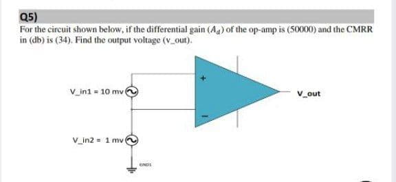
Q5) For the circuit shown below, if the differential gain (Aa) of th in (db) is (34). Find the output voltage (v_out). V_in1 = 10 mv V_in2 = 1 mv ENDI


Q: Q3) For the two stages circuit as shown, find: VIN VOUT CE amplifier CE amplifier Z,- 1 ko Z, = 3 k2…
A: Common Emitter Amplifier-The common emitter circuit configuration is used in many areas of…
Q: Ql:a) Find the overall transfer function C(S) / R(S) for the system shown in figure below using…
A:
Q: Find the gain for the circuit given below. Vio- Vo R
A:
Q: C2 R2 VN Vo R1 Vp RL + Vin
A: First of all, convert the above circuit in the s domain. Thus the circuit becomes:
Q: What are the unity-gain frequency and slew rate of the bipolar amplifier as shown if I1 = 100 μA, I2…
A: Calculating unity gain frequency at I1 = 100 pF
Q: b) Figure Q4 shows the amplifier network. Given the transconductance, gm = 3 mS, gain, Av = - 4, rd…
A: Given the circuit, as shown below: i) We need to draw the high-frequency ac equivalent circuit. ii)…
Q: r circuit below, write the voltage gain (Vout/V1) network transfer function and find the zeros d…
A:
Q: A single-pole op amp has an open-loop gain of 100 dB and a unity-gain frequency of 2 MHz. Find an…
A: Applying KCL to the given circuit
Q: s+10s + K,s²+2s + K2 = 0. where K and K, are feedback gain factors. Determine and plot the region of…
A:
Q: Q10: Obtain the transfer function C(s)/R(s) for the system shown in figure (10). Use 1- Block…
A: from block diagram and signal flow graph..
Q: Find the overall transfer function from the given signal flow graph using Mason's gain formula. Show…
A:
Q: Q10: Obtain the transfer function C(s)/R(s) for the system shown in figure (10). Use 2- Signal flow…
A: Forward paths F1=G1sG2sG3sF2=G1sG2sG7sF3=G5sG6sG3sF4=G5sG6sG7s
Q: What are Amid in dB, fH , fL , and the BW in Hz forthe amplifier described by What type of amplifier…
A: Given As we know, Transfer function of single pole high pass filter
Q: Draw the cascade connection of two amplifiers. Wri
A: the cascaded connection of two amplifiers are shown
Q: A differential amplifier has an output voltage given by Vo =9 Vj-10V2. The two inputs are Vi= 10 mV…
A:
Q: Q10: Obtain the transfer function C(s)/R(s) for the system shown in figure (10). Use ( Signal flow…
A: Solution Using mason's gain formula the transfer can be written as, TF = ∑k=1nMk∆k∆ Where, n is no…
Q: Given a three-stage amplifier that has an input stage with noise ratio = 5 and power gain = 50.…
A: Noise figure- Noise Figure is a measurement which shows the quality of the amplifier. It is…
Q: [CLO2]: In the cascade amplifier shown below, what is the dominant pole that causes the higher…
A:
Q: For the circuit shown below, if the differential gain (A4) of the op-amp is (50000) and the CMR in…
A: CMRR in db = 20 log ((differential mode)/ (common mode gain)). Using above formula we will find…
Q: Define quality factor (Qs) and prove that : Qs = 1/R L/C , what is the quality factor unit.?
A:
Q: (a) What are the worst-case values (minimum or maximum, as appropriate) of the following parameters…
A: The data for AD745 op-amp : Referring the data sheet of the AD745K op-amp. Parameter Conditions…
Q: 2. In the circuit below, the small-signal transconductance of Q2 falls as Vinl-Vin2 rises because…
A: The Expression for transconductance in a BJT network can be given by : gm = IcVt Where, Ic =…
Q: We need to construct an amplifier having Ad= 500 and Bandwidth= 80KHz ..can the uA741 opamp be used…
A: OP-AMP (operational amplifier): It can perform many operations like addition, multiplication., etc.…
Q: Find the expression for the voltage gain for the circuit shown Vc RE VinoKa, o Vout Rc Q2
A:
Q: Answer in detail: Consider that the SNR in dB is equal to 30 dB, what is the actual SNR value (not…
A:
Q: Q5) For the circuit shown below, if the differential gain (Aa) of the op-amp is (50000) and the CMRR…
A: In this question, Find the output voltage of the given CMRR and Ad.
Q: arrangement of all amplifiers in a cascaded form to produce the minimum total noise factor at the…
A: It is given that:
Q: Use a Thévenin equivalent of the left side of the amplifier circuit, shown, to find the current iB.
A: Write the expression for the Thevenin voltage. Vth=R2R1+R2VCC
Q: 2. Find the common-mode gain and V, for the circuit below if Rc = 56k, Rg = 49kn, Vcc 10V, VEE-10V,…
A: As per company guidelines we are supposed to answer only one question. Kindly repost other questions…
Q: Q5) For the circuit shown below, if the differential gain (A4) of the op-amp i in (db) is (34), Find…
A:
Q: 14.) For the difference amplifier circuit, use cireuit analysis (outlined in lecture) to: a. show…
A:
Q: Q3) For the two stages circuit as shown, find: VIN VOUT CE amplifier CE amplifier Z, = 1 kQ Z, = 3…
A: The circuit is as shown below :
Q: Consider the following circuit where Rf =5kΩ Select a value of C to give a bandwidth of 100 rad/sec…
A:
Q: Discussion: 1 How large is the phase shift between Uin and Uout!? 2 How large is the phase shift…
A: "Since you have posted a question with multiple sub-parts, we will solve first three sub-parts for…
Q: Q10: Obtain the transfer function C(s)/R(s) for the system shown in figure (10). Use 1- Block…
A: Note: Since question is not mentioned therefore solving the first one For ther Given block diagram…
Q: The gain margin of a biopotential amplifier whose low-frequency gain 100 is -10 dB. How much must be…
A:
Q: Derive an expression for the output resistance of the Wilson source as shown as a function of the…
A: Given circuit diagram:
Q: Determine the value of small-signal parameter g of Qi for the circuit shown below. Assume Is-6x10⁻¹…
A:
Q: + 1K R7 C3 1NF
A:
Q: Figure bellow shows the response of a system for a step input with magnitude of 15. The initial…
A:
Q: 10(s+4) Y(s) U(s) s(s+ 1)(s + 3)
A:
Q: Q5) For the circuit shown below, if the differential gain (Aa) of the op-amp is (50000) and the CMRR…
A: The given circuit is: Here, The voltage at the non-inverting terminal is: V+=V_in1+V_in2=10+1=11mV…
Q: Using Mason's gain formula calculate the closed-loop transfer function for the system shown below: G…
A:
Q: Refer to the block diagram below. If K = 10, determine the a) overall transfer function, b)…
A: Note :- As per guidelines we are supposed to answer only first 3 sub-parts of a question. So I…
Q: Q2) For the circuit shown in the figure, calculate the input resistance for each step and find the…
A: Given : βDC=100 βac=150
Q: b. Asystem is characterised by a signal flow graph shown in figure 1.Use Mason's gain formula to…
A: Given : In masons gain formula we need forward path gains ,loops, two non touching loops and…
Q: The operational amplifier in the circuit below has the following performance characteristics: Input…
A:
Q: Q3) For the two stages circuit as shown, find: VIN VOUT CE amplifier CE amplifier HE Z,- 1 k2 Z,= 1…
A: The solution can be achieved as follows.
Q: Q5) For the circuit shown below, if the differential gain (A) of the op-amp is (50000) and the CMP…
A:
Q: Q5) For the Channel below, what should be the input distribution that achieves сараcity?
A: The given channel is shown below:


Trending now
This is a popular solution!

Step by step
Solved in 2 steps with 2 images

- For the circuit shown below, if the differential gain (?? ) of the op-amp is (50000) and the CMRR in (db) is (34). Find the output voltage (v_out).Determine the output voltage of an op-amp forinput voltages of Vi1=150μV, Vi2=140μV and CMRRs of100 and 105. (Given Ad =4000) Vd=? Vc=?I need the definitions of the following: •Open loop gain •Input resistance Ri •The output offset voltage (input offset voltage) •The output voltage swing (saturation voltage) •The bias current •The common mode rejection ratio CMRR Please, they can only be from the book "Franco, S. (2005). Design with Operational Amplifiers and Analogue Integrated Circuits.", "González, J. J. and Moreno, A. (2009). Applied Electronic Circuits with Amplifiers Operational", "Carter, B. and Mancini, R. (2009). Op Amps for Everyone" or also "Neamen, D. (2010). Microelectronics: Circuit Analysis and Design" Any of those please
- Suppose the op amp shown has an fT of 3 MHz. What is the phase margin of the amplifier?Consider the active circuit with the schematic:a. Assuming it's an ideal op amp, derive the circuit’s transfer function as a function of frequency, H(jw). Make sure it in canonical form.b. We want a DC gain of 40dB. If the op amp has value of Rin = 10MΩ and Rout = 50Ω, choose appropriate values for R1 and R2. Explain why your selected values of R1 and R2 allow you to ignore Rin and Rout for the remainder of the problem. c. If L = 1H, sketch the straight-line approximation of the Bode plot for the circuit’s gain assuming the op amp can still be considered as ideal.d. The op amp you select turns out to be non-ideal, and it has a real pole at wC = 1krad/s. Write the updated transfer function for your circuit (using your values of R1, R2, and L = 1H). Make it in the canonical form.e. Sketch the straight-line approximation of the Bode plot for the circuit with your updated transfer function from D.Consider the active circuit with the schematic:a. Assuming it's an ideal op amp, derive the circuit’s transfer function as a function of frequency, H(jw). Make sure it in canonical form.b. We want a DC gain of 40dB. If the op amp has value of Rin = 10MΩ and Rout = 50Ω, choose appropriate values for R1 and R2. Explain why your selected values of R1 and R2 allow you to ignore Rin and Rout for the remainder of the problem.
- The open-loop gain A of real (nonideal) op-amps isvery large at low frequencies but decreases markedlyas frequency increases. As a result, the closed-loopgain of op-amp circuits can be strongly dependent on frequency. Determine the relationship between a finiteand frequency-dependent open-loop gain AV(OL)(ω)and the closed-loop gain AV(CL)(ω) of an invertingamplifier as a function of frequency. Plot AV(CL)versus ω. Notice that −RF/RS is the low-frequencyclosed-loop gain.Show the manual solution for the simulated values of the multistage op amp below. Vcc= 12VQ4/A)- Show the connection of three combination op-amp stages using an LM348 IC to provide outputs that are 110, 1681, and 420 times larger than the input. Use a feedback resistor of Rf = 400 k? in all stages, while can use only (R= 40 k? for first stage), (R= 10 k? for second stage), and (R= 20 k? for third stage
- Show the connection of three combination op-amp stages using an LM348 IC to provide outputs that are 110, 1681, and 420 times larger than the input. Use a feedback resistor of Rf = 400 k? in all stages, while can use only (R= 40 k? for first stage), (R= 10 k? for second stage), and (R= 20 k? fot third stage)Consider the active circuit:a. Assuming it's an ideal op amp, derive the circuit’s transfer function as a function of frequency, H(jw) in canonical form.b. We want a DC gain of 40dB. If the op amp has value of Rin = 10MΩ and Rout = 50Ω, choose appropriate values for R1 and R2. Explain why your selected values of R1 and R2 allow you to ignore Rin and Rout for the remainder of the problem.The upper critical frequency of an op-amp’s open-loop response is 200 Hz. If the midrange gain is 175,000, answer the following: What is the ideal gain at 200 Hz? What is the actual gain? What is the op-amp’s open-loop bandwidth?