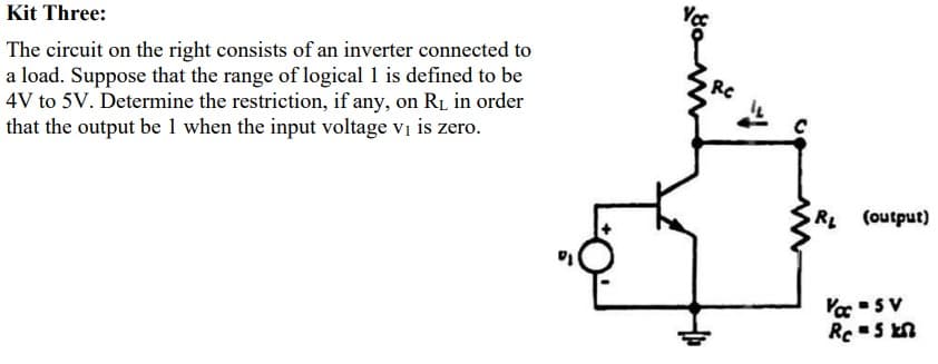
The circuit on the right consists of an inverter connected to a load. Suppose that the range of logical 1 is defined to be 4V to 5V. Determine the restriction, if any, on RL in order that the output be 1 when the input voltage vi is zero.


Q: Design a reference inverter to achieve a delay of 250 ps when driving a 0.2-pF load using a 3.3-V…
A: Assuming Kn = 100 μA/v2 and Kp = 40 μA/v2 Also,
Q: F=A+B'C+A'BC' I need to construct the circuit in multism with an inverter, and gate, or gate.
A:
Q: α
A:
Q: The load voltage waveform of a single phase full bridge inverter supplied fr source is shown in…
A: Rectifier: Because nearly every electrical appliance runs on DC (Direct Current), the rectifier…
Q: 3. A) Use a 8-to-1 multiplexer and an inverter to implement the function: F(a,b,c,d) =…
A: As per guidelines these are not interlinking these are two different questions.i have attempted…
Q: Required information A resistive load inverter in two logic states is given as follows: Vpp Ipp R R…
A:
Q: Draw the circuit diagram and output voltage and current wave shapes of a full-bridge inverter with…
A: The inverter is a circuit that converts DC power into AC power at the required voltage and…
Q: The logic swing in the inverter as shown is reducedby a factor of 3 by reducing the value of RCand…
A: Calculating collector resistance RC’ Calculating logic swing voltage
Q: a) When the output voltage of a static CMOS inverter just begins the transition from a high output…
A: According to guidelines we need to solve only the first three subparts. according to the question…
Q: Find the transfer functions for the two systems shown in Figure (E.(S)/E(S)). R2 E'(s) EAN) E(s)…
A: In this question we will find transfer functions...
Q: 2-a 2 -V& mini An inverter which produces the output voltage shown the figure above is used to…
A: First derive the expression for fundamental output voltage and than find the firing angle to get…
Q: Am trying to design a pure sign wave dc to ac inverter, from what you know, make known to me three…
A: The common use of an inverter is for the conversion of Direct current supply to Alternating current…
Q: 7- A single-phase inverter produces an output voltage with fundamental Vo,1=220V and 47HZ. The load…
A:
Q: Design a CMOS logic gate
A:
Q: Invert the output of the circuit built in task-1? Use Nor gate as an inverter.
A: The solution can be achieved as follows.
Q: 2. A Half-bridge inverter with resistive load and capacitive elements is given in the figure. Vb…
A: A half-bridge inverter is a device that converts DC voltage into AC voltage. It consists of 2…
Q: Justify the usage of the RCD (residual current device ) at the AC side of the inverter? You have to…
A: Residual current device (RCD) - An RCD is a smart safety feature that immediately turns off the…
Q: A Half-bridge inverter with resistive load and capacitive elements is given in the figure. Vb = 96V,…
A: The detailed answer is solved below according to the given parameters and instructions in the…
Q: Design the following circuits as shown in the block diagram Ac inverter de de var ACOVA f = Var…
A: A shift register is a type of digital memory found in calculators, computers, and data processing…
Q: 47 For the inverter of Figure P10.47, Rg = 5 k2 and Rci = Rcz = 2 kS2. Find the minimum values of ß1…
A:
Q: Doe Do Dor Do Vị V3 Figure 2: Simulating delays with inverters. Let each inverter have delay A, then…
A: Given the logic circuit as shown below: We need to construct this circuit using the MUX circuit. We…
Q: For an inverter circuit where the load is RL circuit, the value of Zn, and In increase as n…
A: Need to find true or false
Q: V. 2x-a 2 -V ek An inverter which produces the output voltage shown the figure above is used to…
A:
Q: 2) Find VH, VL, and power dissipation (for vo = V1) for the logic inverter with saturated load in…
A:
Q: LS373 A7 OC A0 Y
A:
Q: How Buck-converter could be converted into an inverter ? Justify your answer with drawing
A: Buck-converter - A buck converter is a DC-to-DC power converter that reduces the voltage from source…
Q: Design a CMOS logic gate
A:
Q: Draw the schematic for a four-input NOR gate witha saturated load device. What are the W/L ratios…
A: Concept: The simplest area calculations are for squares and rectangles and to find the area of a…
Q: Design a pseudo NMOS inverter to operate fromVDD = 3.0 V with VL = 0.3 V and a power of200W. (b)…
A: Given VDD=3 VVL=0.3 VP=200 W If the power in watts then the width-to-length ratio will be very high…
Q: An inverter with a resistive load, VDD = 3.3 V, P = 0.1 mW, VL = 0.2 V, K'n = 60 UA/V2 and VT N =…
A: Solution- Given,VDD = 3.3 VP = 0.1 mWVL = 0.2 VKn' = 60μA/V2VTN = 0.75 V Let transistor operate in…
Q: Design an adder circuit which adds (Ce or (12),g in decimal to the 1's complement of a generic 4-bit…
A:
Q: 1. A square-wave inverter has an R-L load with R=15 2 and L=10 mH. The inverter output frequency is…
A:
Q: (k=45V;=0,75V,Voo=5V;R;=100KS ) VIL=0,972V VDD RL R. OUT IN
A: Consider the first resistive load inverter. By applying Kirchhoff's voltage law, the following…
Q: 1. Five identical inverters are connected in a chain. The low-to-high propagation delay of the…
A:
Q: 4) Find VH, VL, and power dissipation (for vo= V1) for the logic inverter with linear load inverter…
A:
Q: Draw the schematic circuit for a CMOS inverter and the relative voltage transfer characteristic…
A: “Since you have asked multiple question, we will solve the first question for you. If you want any…
Q: (a) What is the power-delay product for the inverter in Prob. 7.29? (b) Estimate the maximum switch-…
A: Given,For a symmetrical CMOS inverter - WLN=21WLP=51C=0.20 pFVDD=3.3 VVTN=0.75 VVTP=-0.75 V
Q: . Implement the following circuit using components for an and gate, an or gate, and an inverter.…
A: Given the following the circuit as shown below: We need to write the code for circuit…
Q: An inverter must drive a 5-pF load capacitance with τp = 1 ns. Scale the reference inverter to…
A: Given τp=1 nsCL=5 pF Calculating average propagation delay τp=1.2RonnCLRonn=τp1.2CLRonn=1 ns1.2×5…
Q: Do the circuits of the systems listed as examples of SINGLE-INPUT-SINGLE-OUTPUT (SISO) 1. (The…
A: Consider the circuit shown below. In the above circuit, it works as the inverter for the high input…
Q: An 8-bit A/D converter-type inverter has 500 kHz clock. Find (a) maximum conversion time, (b)…
A: We have been given an 8-bit A/D Converter-type inverter with, Frequency (F) = 500 KHz = 500 * 103 Hz…
Q: a) A standard TTL inverter gate is shown in the figure. The supply voltage is 5V. Calculate the…
A: Solution (a) - When Vi =0.1 V Thus, when the input voltage is 0.1 V than output voltage is 4.28 V.
Q: 1- The region of operation of MOSFETM MD at v = 4.2V is %3D 2- The region of operation of MOSFETM ML…
A: We need to tell about region of operations of both MOSFET .we know condition for MOSFET to work in…
Q: Implement the following function using 4-input CMOS gate and an inverter? (A+B) (C+D)
A: Given inputs to the CMOS gate are A, B, C, and D We have to implement the function F=A+BC+D using…
Q: An inverter which produces the output voltage shown the figure above is used to supply the series R…
A: Given data, Output voltage for fundamental frequency is given, V01=25 V DC input voltage is given,…
Q: For designing a circuit which adds two 10-bit numbers and then complements the sum, which of the…
A: For adding two 4 bit numbers we require 4 Full adders. So that for designing a circuit which adds…
Q: basic electronics please give full naswer thanks Using MOSFET design your own circuit such that it…
A:
Q: 1) Half wave bridge inverter have following construction find the output signal sequencly depending…
A: Half bridge inverter Vs=60 V Assumptions: 1. Type of load are not specified. We assume resistive…
Q: Identify the various conversion stages within the topologies and what functions8 they fulfill( wave…
A: An inverter that converts the DC output voltage and converts it to AC and uses the battery system…

Step by step
Solved in 2 steps with 1 images

- Implement F(A,B,C)= m2+m5+m6+m7, using the smallest possible multiplexer and inverters as needed.Q1: Design a combinational circuit with four inputs lines that represent a decimal digit in BCD and four output lines that generate the 9’s complement of the input digit. Q: 2 Show how a full adder can be converted to full-subtractor with the addition of one inverter circuit.Draw the schematic for a four-input NOR gate witha saturated load device. What are the W/L ratios ofall the transistors, based on the reference inverter ? (b) What is VL if all the logic inputs are equal to 1?
- Five identical inverters are connected in a chain. The low-to-high propagation delay of the inverter is 12ns while the high-to-low propagation delay is 10ns. The input at the first inverter is changed from 1 to 0 at time t=0ns. How long will it take before the output of the 5th inverter change from 0 to 1?If,for a single phase half bridge inverter the amplitude of output voltage is Vs and the output power is P then their corresponding values for a single phase full-bridge inverter are a. 2Vs,2P b. 2Vs,4P c. 2Vs,P d. Vs,PF=A+B'C+A'BC' I need to construct the circuit in multism with an inverter, and gate, or gate.
- Calculate the fanout for the ECL inverter as shown at room temperature for βF = 30. Definethe fanout N to be equal to the number of invertersfor which the VH level deteriorates by no more thanone VT . (Hint: At vO2, VH = VBE4 + iB4RC.)Do we need to consider the case for vO = VL?Why?Wire delay I. Calculate the delay of a 10 mm wire in 28 nm technology that is divided into 20 0.5 mm segments with a 20× minimum-size inverter driving each segment.1. A square-wave inverter has an R-L load with R=15 Ω and L=10 mH. The inverter output frequency is400 Hz (fundamental frequency).(a) Determine the values of the required to establish a load current which has a fundamentalfrequency component of 10 A rms with α = 0.(b) For a controlled full-bridge inverter, the dc source is 125 V and the switching frequency is60 Hz. Determine the value of α to produce an output with amplitude of 100 V at the fundamentalfrequency.
- When Inverters are used as the input to a NAND gate, the circuit performs what logic function? When Inverters are used as the input to a NOR gate, the circuit performs what logic function? A point in a logic circuit labelled STB3 can assume which of the following states ? a.binary 0 b.binary 1 c.either binary 0 and 1Hello, I don't konw how to implement expression for part(b) with NAND and NOR gate. My method is : (1) Implement these expression with AND and OR gate. (2) Add bubble in front of the AND gate and add bubble behind the OR gate.Is there anything wrong with my method? Besides, I am wondering why there is a inverter behind the NAND gate (shown in answer1.PNG)Thanks.Plot a graph of the overall voltage transfer characteristic for two cascaded inverters if each individual inverter has the voltage transfer function definedin . (b) Repeat for 10 inverters.