the donor ConCentration Concentration is the acceptor the resulting Semiconductor would be the intrinsic Concen tration is the hole Con Centration is
the donor ConCentration Concentration is the acceptor the resulting Semiconductor would be the intrinsic Concen tration is the hole Con Centration is

Chemistry: The Molecular Science
5th Edition
ISBN:9781285199047
Author:John W. Moore, Conrad L. Stanitski
Publisher:John W. Moore, Conrad L. Stanitski
Chapter19: The Chemistry Of The Main-group Elements
Section: Chapter Questions
Problem 74QRT

Related questions
Question
I need the answer as soon as possible
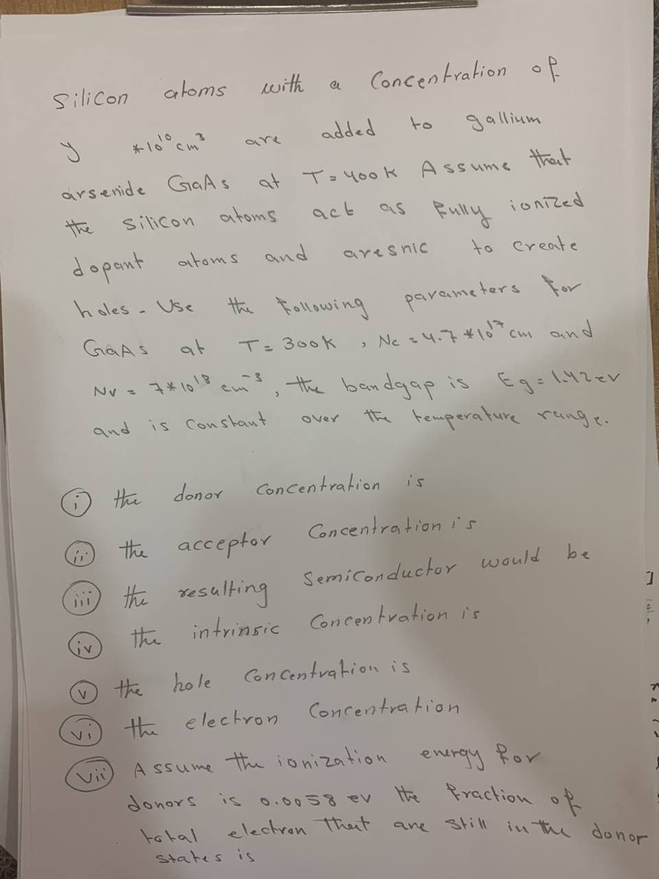
Transcribed Image Text:Silicon
atoms
with
Concentration o.
*10 cm
added
to
gallium
are
arsenide GaAs
at Toyook
A ss ume
that
silicon atoms
act
as
Fully ionized
the
dopant atom s and
to create
aresnic
the Following Pparame ters For
at
holes - Use
Tz 300k
, Ne z4.7*10 cm and
the bendgap is Eg:l.42ev
the temperature range.
and
is Constant
over
the
donor
Concentration
is
Cencentration is
the acceptor
O the resulting Semiconductor would be
Concen trationi's
the
intrinsic
歩 hole
Con Centration is
the elechron
Concentra tion
A ssume the ionization enerqy Ror
Vi
donors is 0.00 58 ev
the fraction of
electran thut
ane Stil
in the donor
States is
Expert Solution
This question has been solved!
Explore an expertly crafted, step-by-step solution for a thorough understanding of key concepts.

Step by step
Solved in 5 steps

Knowledge Booster


Learn more about
Need a deep-dive on the concept behind this application? Look no further. Learn more about this topic, chemistry and related others by exploring similar questions and additional content below.Recommended textbooks for you
Chemistry: The Molecular Science
Chemistry
ISBN:
9781285199047
Author:
John W. Moore, Conrad L. Stanitski
Publisher:
Cengage Learning
Chemistry: The Molecular Science
Chemistry
ISBN:
9781285199047
Author:
John W. Moore, Conrad L. Stanitski
Publisher:
Cengage Learning