1.1 List the truth table with 16 binary combinations of the four input variables. Then list the binary values for T1 through T4 and outputs F1 and F2 in the table. 1.2 Redesign the logic circuit if F1 and F2 using (a)NAND gates only and (b) NOR gates only. A T3 В C F1 T2 T4 D F2
Q: 1. Consider the following function: Hint: do not simplify F = [ml(y+ x)] + (1 + nm)(xOz') a.…
A: Explanation: a. F = [ (ml)' (y+x) ] + (l+nm) (x⊕z') Now the complement of F is F' = { [ (ml)' (y+x)…
Q: Simplify the given Boolean function and design its logic gates(NAND and NOR) with the help of…
A: Simplify the given Boolean function and design its logic gates(NAND and NOR) with the help of…
Q: if332to base10=x to base8 then find the value of X.(c)1001011.0112 to equivalent decimal
A:
Q: 1- Convert the following logic gate circuit into a Boolean expression. Write Boolean subexpression…
A:
Q: A combinational circuit with three inputs (A, B and C) generates the 2’s complement of the input…
A: The required logic circuit can be designed by using the given condition and the reduced Boolean…
Q: Build the logic circuit for the function F1 = XYZ + YŽ + YZ using PAL
A:
Q: (b) Design the state diagram and state transition table for the state table in Table 1. Hence,…
A:
Q: Consider the following logic circuit [Figure Q18(c)]. Construct the truth table for the output…
A:
Q: 3. Minimize the Booklean function using Boolean algebra rules and realise the logic eircuit using…
A: 1. The given algebraic equation is, F=AB+BC+BC+AB And it is reduced to F=AB+BC+BC+AB =AB+AB+BC+BC…
Q: Question No. 1: Design Logic diagram using Universal gates (either NAND, NOR) only for the given…
A: K-map is used to minimize the expression . It is represented as table of rows or columns having…
Q: Question 1 a) 0 0 1 0 1 1 0 1 1 1 0 0 ! 0 0 1 0 1 1 1 Y 0 1 1 1 0 0 0 a b C d e f Figure 1 As shown…
A: Brief description: From the given timing diagram we need to write the logic circuit. In the…
Q: Simplify the given Boolean function and design its logic gates(NAND and NOR) with the help of…
A: Simplify the given Boolean function and design its logic gates(NAND and NOR) with the help of…
Q: Generating truth table for the following logic statement: (A NOR B) NAND (B OR C OR D) NAND (A XOR…
A:
Q: Given the following functions: - F(A,B,C)= (A + B)(A+ AB') + AB+ A+ Z (A,B,C)= A'C' + ABC + AC' B.…
A: Dear student as per our guidelines we are supposed to solve only one question in which it should…
Q: For Design a combinational circuit with 4-inputs and 4-outputs. The output generates the 2’s…
A: Truth Table: Minimized expression using K-map: S1) S1=AB+AC+AD+ABCD S2) S2=BC+BD+BCD S3)…
Q: Question 1 f J: The figure below is the logic diagram of a special counter. D flip-flop OD to D…
A: We need to find state diagram .
Q: 2. What is the largest binary number that can be expressed with 16 bits? What are the equivalent…
A: Note: We are authorized to answer one question at a time, since you have not mentioned which…
Q: ) Assume A=A3A2A1A0, and B=B3B2B1B0 , both 4 bit binary numbers. If Y=3A+B, answer the following:…
A: First, we will implement a circuit for the binary multiplication of 3A. The implementation for the 2…
Q: 21. A = {1, 3, 5, 7, 9, 11, 13) and B = {1, 3, 7, 11). What would be the output of a logic gate that…
A: To solve above problem, one should understand AND, OR and NOT gate. For AND gate An AND gate will…
Q: Create a TRUTH TABLE, and draw the equivalent LOGIC DIAGRAM and TIMING DIAGRAM of the following…
A:
Q: 2. Consider the following operation: Z = AB BC a. Write out the truth table for the given…
A: Given operation Z = AB.BC The truth table, logic circuit and the implementation…
Q: 2. B. SR Master-Slave Flip-Flop a. Draw the logic diagram of SR master-slave flip-flop and implement…
A: Given, SR master slave flipflop: Y is output of master latch, Q is output of slave latch.
Q: Design a combinational circuit with four inputs and one output. The output is 1, when the binary…
A: as per instruction we must solve the first question only. if you want answer for other subparts…
Q: Question 1 Simplify a logic function F(a,b,c,d) = a'b'cd + a'bd + bc'd' + ab'c'd' assuming that the…
A: Given logic functionF(a,b,c,d)=a'b'cd+a'bd+bc'd'+ab'c'd'a=c=1 is don't care
Q: 5. Draw the logic circuit for the function f = y'z' + x'y' + x'y'z'
A: Given, f=y'z'+x'y'+x'y'z'
Q: The block diagram and the logic symbol of a 4-bit parallel adder are shown below. Using the logic…
A:
Q: Simplify a logic function F(a,b,c,d) = a'b'cd + a'bd + bc'd' + ab'c'd' assuming that the network…
A: To solve above problem one should have basic understanding of Boolean expression: Some basic…
Q: Figure 3 Figure 1 21 21 DE Figure 4 Figure 2 21 Figure 5 JSE THE TRUTH TABLE TO JUSTIFY THE LOGIC…
A: Given With the help of truth table for all the given figures we calculated the output equation…
Q: Simplify the given Boolean function and design its logic gates(NOR) F3(x,y,z) =…
A: 1) Given expression, f3x,y,z=x'yz'+y'z+x'z'
Q: Problem / Draw each expression the logic gate 1 X = ABC + ABC + ABC + ABE @ X= (A+B) (C+D) (E+F) (3)…
A:
Q: The function z =(A+C) + BC+ (AC+D) a) Show the truth table of z. b) Implement this the logic…
A: The given Boolean expression can be implemented by using the multiplexer. The three inputs can be…
Q: Q1: Answer the following questions: 1) The hexadecimal number Al' has the decimal value equivalent…
A: 1) option B is correct. The detailed solution is provided below.
Q: 4. Draw the logic diagram corresponding to the following Boolean Expression. a) (P+ R)• (Q ® R))+ (P…
A:
Q: Draw the logic diagrams for the following Boolean expressions: (a) Y= A'B' +B (A+ C) (b) Y= BC +AC…
A:
Q: What is the simplified algebraic expression for the logic gate shown? X xa Y OX + Y OX.Y OX.Y ΟΧΘΥ…
A: Given, The logic gate,
Q: 3. For the circuit shown below answer the following. (a) Determine the Boolean expression for the…
A:
Q: Draw the logic diagrams for the following Boolean expressions: (a) Y=A'B' +B (A+ C) (b) Y= BC + AC'…
A: As mentioned by the student we have to solve the questions c and d.
Q: Fill in the blanks in the truth table of the given digital circuit. Use for NOT gate egX. Use…
A: Here 7 gates were used Gate 1 AND gate Inputs X, Y, Z output = XYZ
Q: 4. Implement the following logic function by using a 74HC151 data selector. F(A,B,C,D) = ACD + ABD…
A:
Q: You must produce all seven truth tables (AND, OR, NOT, XOR, NAND, NOR and XNOR) and an eight truth…
A: OR gate # Function to simulate OR Gatedef OR(A, B): return A | B print("Output of 0 OR 0 is",…
Q: Draw the logic gate, its Boolean expression and its truth table for the gates below: -…
A:
Q: Complete the design for the state machine described in the state diagram below and Write out the…
A: I have explained in detail
Q: 3/ Select a logic gate which is alone enough to implement any boolean expressions. AND gates NOT…
A:
Q: Label all outputs and compule the truth table for the follewine logic aircuit: A B
A: AND gate: An AND gate is a logic gate having two or more inputs and a single output. If all inputs…
Q: Half-subtractor is a combinational circuit capable of subtracting a binary number from another…
A:
Q: Draw a block diagram, truth table and logic circuit of 1*16 Demultiplexer and explain its working…
A:
Q: REPRESENTATION OF LOGIC EXPRESSION Example 3. Write the logic expression and obtain the truth table…
A:
Q: Given a 4-bit signed input P=P3P2P1P0 and a control input Z, use a 4-bit adder and any logic gates…
A:
Please show complete solutions. Thank you.
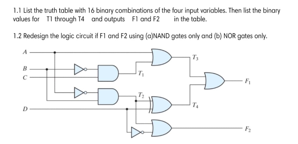
Trending now
This is a popular solution!
Step by step
Solved in 5 steps with 5 images
- Design 2 bits counter that count down by using T flip flop when input x =1 and counts upwhen x=0. Find the following1. Derive the state table2. Derive the K‐map simplifications.3. Draw the logic diagramDraw a block diagram, truth table and logic circuit of 1*16 Demultiplexer and explain its working principle.Give the output of the logic gate for the given inputs.3. OR Gate: A = 1, B = 1, C = 0
- Use Digital Logic Simulator Fill-in the blank boxes with the correct LOGIC GATE/ Full/Half AdderFrom the following truth table: i) Construct Karnaugh Map (SOP)ii) Design combinational logic circuit using 2-input NAND Gateiii) Design combinational logic circuit using 4:1 Multiplexer) Assume A=A3A2A1A0, and B=B3B2B1B0 , both 4 bit binary numbers. If Y=3A+B, answer the following: Design a digital circuit that implements Y using the minimum hardware. You may use 4 bit adders, Half adders, Full adders, and a minimum number of logic gates as necessary. *(sketch your solution)
- 1) Design the logic gates that compare (3) bit binary numbers that are "equal" or "not equal." A0 B0 A1 B1 A2 B2 2) Derive the logic equations for both outputs 3) What type of circuit/system can this be used in an application you could create?Given the logic function: F(A,B,C,D) = Σm(0,4,5,10,11,13,14,15) a. Find a minimum circuit which implements F using AND and OR gates. Identify two 1-hazards in the circuit. b. find another minimum circuit which implements F using AND and OR gates. Identify two 0-hazards in the circuit. c. Find an AND-OR circuit for F which has no hazards.AND OPERATION 1. In your own words, what is a logic circuit? 2. What is the largest number of inputs which a single TTL IC can have constructed from the AND gates in the 7411 IC?
- Design a three bit synchronous binary counter that counts two by two with T-flipflops,continously. Output should be one when the counter equals maximum number.a. Draw the exitation table b. Draw the corresponding state diagram. c. Tabulate the state table for the sequential circuit. d. Draw the logic diagram of the circuit.Design a 4-bit arithmetic circuit, with two selection variables S1 and S0, that generates the arithmetic operations in the following table. Draw the logic diagram for a single bit stage. Note that B’ represents “Not B”. Draw the logic diagram for a single bit stag(a) Differentiate comparatively the analogue and digital representations. (b) If 33210= Xs then find the value of X. (c)1001011.0112 to equivalent decimal (d) What do you know about the logic gates? Explain the AND gate in details. 410 A