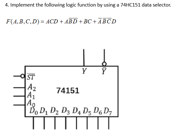
4. Implement the following logic function by using a 74HC151 data selector. F(A,B,C,D) = ACD + ABD +BC + ABCD ST A2 A1 74151 | Ďo D1 D2 D3 D4 D5 D6 D7 TIT


Q: A combinational circuit with three inputs (A, B and C) generates the 2’s complement of the input…
A: The required logic circuit can be designed by using the given condition and the reduced Boolean…
Q: Simplify the Boolean function and design its logic gate. B (x, y, z) = X’Z+X’Y+YZ
A: The function given in question is a three-variable function with inputs as “X”, “Y” and “Z”. To…
Q: Q1. Design a 4-bit arithmetic logic circuit that perform the arithmetic logic operation below: S2 |…
A: Arithmetic Logic Unit is a common operational unit with number of storage registers connected to it,…
Q: 18. Derive the Boolean expression for the logic circuit below: a. CA + CB +CD A B b. C(A + B)D с.…
A:
Q: (a) Minimise the following logic function using the Karnaugh maps method: f(x, y, z) = x'y'z' + x'y…
A:
Q: Consider the following logic circuit [Figure Q18(c)]. Construct the truth table for the output…
A:
Q: Determine the truth table for the following logic circuit. Then identify the type of logic gate…
A: Given a logic circuit and we need to evaluate its truth table and type of logic gate Lets give the…
Q: library IEEE; use IEEE.STD LOGIC 1164 ALL; entity dec2to4 is Port ( enable : in STD LOGIC; sw : in…
A: Digital electronics
Q: 3. Minimize the Booklean function using Boolean algebra rules and realise the logic eircuit using…
A: 1. The given algebraic equation is, F=AB+BC+BC+AB And it is reduced to F=AB+BC+BC+AB =AB+AB+BC+BC…
Q: 61 Design a combinational logic circuit that accept (4-bit) binary number (A) and generate an output…
A: Note: As per the company guidelines, we experts are allowed to answer only 3 subparts. Kindly post…
Q: 6. i) For the circuit shown in Figure Q16, Find the logic functions of X and Y Figure Q16 ii)…
A: We need to write the expressionfor logic circuit and need to simplify it.
Q: (a) Study the sequential circuit constructed by two D FFs with an active-high synchronous reset in…
A: Flip flop is a latch with additional control input (clock or enable ). A flip flop is used to store…
Q: For the given function P P(A,B, C, D) =Em (0,1,2,4,6,7,8,9,10,11,12) + d (3,13,15) a. Simplify P…
A: To solve above problem, one should know about k-map. K-map is used to minimize the Boolean…
Q: 4.1 Reduce the following Switching Function equations by using a Carnoh diagram and writing a Logic…
A: Reduce the given expression using K- map ?
Q: Open ended task: Construct the logic for 4-bit binary adder-subtractor using 4-bit parallel adder…
A: So we will develop a logic for 4 bit binary adder-subtractor using 4 bit parallel adder and X-OR…
Q: Using three MSI circuits, construct a binary parallel adder to add two 12-bit binary numbers. Label…
A: We need to design a binary parallel adder to add two 12 bit binary numbers.
Q: For the given function P P (A, B, C, D) =∑m (0,1,2,4,6,7,8,9,10,11,12) + d (3,13,15) a. Simplify P…
A:
Q: ) Assume A=A3A2A1A0, and B=B3B2B1B0 , both 4 bit binary numbers. If Y=3A+B, answer the following:…
A: First, we will implement a circuit for the binary multiplication of 3A. The implementation for the 2…
Q: 5. A) Design the following Boolean function using a 3-to-8 line decoder and an OR gate. F(A,B,C) =…
A: Since you have asked multiple questions, we will solve the first question for you. If you want any…
Q: Q 5. Determine the expression of the given logic circuit and simplify it. (using De'Morgan's law /…
A: NOR Gate NOR gate is a type of universal gate in which when all the inputs are low then the output…
Q: ways to speed up ripple Mark all that apply. Use faster logic gates. Oa. O b. Eliminate the output…
A: Ways to speed up Ripple adders is explained in the below step
Q: Q4 A-Design Parallel load/Shift right 4 bit register with LD/SR signal. If LD/SR =1 then register…
A: Note: As per Bartleby guidelines, solution for only first question is provided, You are requested to…
Q: Question: A combinational circuit is defined by the following three Bollean function…
A: The implementation is as follows.
Q: Derive the hazard free Boolean expression for given logic function.…
A: The given expression is in the SOP (sum of products) form. 0 - 0000 4 - 0100 5 - 0101 10 - 1010 11 -…
Q: 5. Draw the logic circuit for the function f = y'z' + x'y' + x'y'z'
A: Given, f=y'z'+x'y'+x'y'z'
Q: • 6.7 Show how to build each of the following logic functions using one or more 74x138 binary…
A: As mentioned in the question to solve the part A and part F. In question it is required to design…
Q: 1)For the function given as f (X1 , X2 , X3 , X4 ) X1 , X2 will be defined as selection inputs and…
A:
Q: Simplify a logic function F(a,b,c,d) = a'b'cd + a'bd + bc'd' + ab'c'd' assuming that the network…
A: To solve above problem one should have basic understanding of Boolean expression: Some basic…
Q: Im. d) Write Y = f(w, x, y, z) in SOP form. e) Draw the SOP logic circuit. f) Write Y = f(w, x, y,…
A:
Q: The function z =(A+C) + BC+ (AC+D) a) Show the truth table of z. b) Implement this the logic…
A: The given Boolean expression can be implemented by using the multiplexer. The three inputs can be…
Q: (a) Study the sequential circuit constructed by two D FFs with an active-high synchronous reset in…
A: D flip flop is delay flip flop. It has one input and one output. The truth table of T flip flop is…
Q: Draw the full logic diagram of an octal-to-binary priority A (LSB) 1+3+5 +7 1.2 .+3..+ B -…
A: Let D0 to D7 be the inputs of the priority encoder. Write the truth table for the above encoder.…
Q: Simplify the given Boolean function and design its logic gates(NAND and NOR) F4(x,y,z) = x’y’+xz+x’z
A: Simplify the given Boolean function and design its logic gates(NAND and NOR) F4(x,y,z) = x’y’+xz+x’z
Q: Q2 A) Starting from Ex-OR (SOP) expression: a- develop Ex-NOR (SOP) expression. A O A=... b- Find AO…
A: To get the SOP expression for EX-NOR gate
Q: Show the Ladder logic program and the equivalent Function Block Diagram for the following Boolean…
A: Solution (1) Y=(A+B)·(C+D⊕A)·A The functional block diagram we will have for the given boolean…
Q: DESIGN 1-6 SYNCHRONOUS UP COUNTER USING JK FLIP-FLOP 7476 IC REQUIRED: A) EXCITATION TABLE OF JK F-F…
A: The solution is given below
Q: Q3) a- Draw the logic diagram for a circuit that will divide the (fcLK) by 32. Use (+ve) edge…
A:
Q: Course: Digital logic design DLD Please solve it on emergency basis: Express the following…
A:
Q: A) Draw a frequency divider "divide by 2" and 'divide by 4 logic circuits as a single circuit…
A: According to the question, we need to design the "Divide by 2" and "divide by 4" circuit by JK FF.…
Q: b) Implement this the logic function (z) using the multiplexer 74HC151 shows in the picture Note:…
A: We need to design the given Boolean function by using of given mux .
Q: **Note: Answer Four Qucstions Only Q1) Design a full Subtractor circuit that performs the…
A: The digital circuits can be combinational as well as sequential circuits. The combinational circuits…
Q: Q16. i) For the circuit shown in Figure Q16, Find the logic functions of X and Y A Figure Q16 ii)…
A: We need to find the output of the given logic circuit and simplified expression of it.
Q: A 2-to-4 line Binary Decoder converts coded inputs into coded outputs. i) Find the decoded output…
A:
Q: 1. Using a single 3-to-8 decoder, design the logic circuit to realize the following Boolean…
A:
Q: Kindly Answer What is the internal structure of 7483 IC? What do you mean by code conversion? What…
A: We are authorized to answer three subparts at a time since you have not mentioned which part you are…
Q: a. F1 = X + XỸ + ZY b. F2 = XY + X + XYZ с. FЗ 3D АВС + АВС + AВС d. Draw the circuits for…
A:
Q: Show the Ladder logic program and the equivalent Function Block Diagram for the following Boolean…
A:
Q: O Consider the table given below in which A, B, C, and D are input variables. F is the output…
A: The solution can be achieved as follows.
Q: REPRESENTATION OF LOGIC EXPRESSION Example 3. Write the logic expression and obtain the truth table…
A:


Trending now
This is a popular solution!

Step by step
Solved in 2 steps with 2 images


- I was able to fill out the truth table for part A. I ONLY need help for PART B. B) Implement the logic function (z) using the multiplexer 74HC151 shows in the picture.) Assume A=A3A2A1A0, and B=B3B2B1B0 , both 4 bit binary numbers. If Y=3A+B, answer the following: Design a digital circuit that implements Y using the minimum hardware. You may use 4 bit adders, Half adders, Full adders, and a minimum number of logic gates as necessary. *(sketch your solution)2. Design 6 lines to 64 lines Decoder using IC# 74138. You can use other logic gates/IC, if necessary.
- . Design a combinational circuit to convert a 4-bit binary number to gray code using(a) standard logic gates,(b) decoder,(c) 8-to-1 multiplexer,(d) 4-to-1 multiplexer.Simplify the given Boolean function and design its logic gates(NAND and NOR) F4(x,y,z) = x’y’+xz+x’zchoose the correct answer Logic gates from which of the following logic families are suitable for VLSI circuits? a. MOS b. ECL c. CMOS d. TTL
- Simplify the Boolean function and design its logic gate. B (x, y, z) = X’Z+X’Y+YZConvert the binary number (1011101) to its equivalent decimal and BCD values. (Show you work) Convert the decimal number (478) to its equivalent hexadecimal and binary values. (Show you work) List the next twenty five hex numbers in sequence from (9E7) hex upwards, adding one each time. (Write them horizontally, with comma as separator) Answer the following logic operations : a) 0 . Z’ = b) 1 + W = c) d . d’ = d) b . b = e) X + (X+1)’ = f) 1 + X’ = g) C + B’C’ = h) B + (BC)’ =…3. Simplify F(A;B;C;D) = summation (1; 3; 8; 10) d(A;B;C;D) =summation (0; 2; 9). Draw an all-NOR logic diagram for the simplified function.
- From the following truth table: i) Construct Karnaugh Map (SOP)ii) Design combinational logic circuit using 2-input NAND Gateiii) Design combinational logic circuit using 4:1 MultiplexerDraw a block diagram, truth table and logic circuit of 1*16 Demultiplexer and explain its working principle.Implement the following logic function using only 3-8 decoders and logic gates. f(a,b,c,d ) Σ m(2,4,6,8,10,14,15)