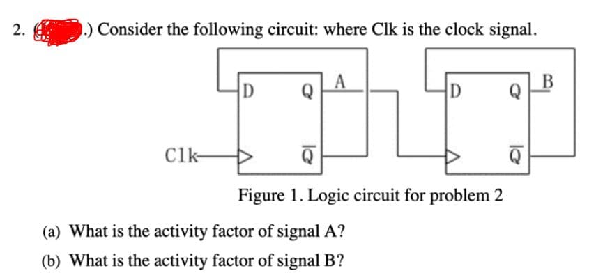
2. Consider the following circuit: where Clk is the clock signal. В D Q D Clk- Figure 1. Logic circuit for problem 2 (a) What is the activity factor of signal A? (b) What is the activity factor of signal B?


Q: 1. Consider the following function: Hint: do not simplify F = [ml(y+ x)] + (1 + nm)(xOz') a.…
A: Explanation: a. F = [ (ml)' (y+x) ] + (l+nm) (x⊕z') Now the complement of F is F' = { [ (ml)' (y+x)…
Q: A manufacturing plant needs to have a horn sound to signal quitting time. The horn should be…
A: Representing the events by alphabets as shown below: O-Horn Activated A-After 5 o’clock B-Machines…
Q: Select a suitable example for for combinational logic circuit. O a. None of the given choices O b.…
A: The given questions are from the digital electronics subject. A circuit which remains unaffected by…
Q: Construct the Logic Circuirs
A: The function is given as, X=W+PQ-
Q: Q1 (a) Write the boolean expression of the combinational digital circuit shown in Figure 1. F :D…
A: Given:
Q: 1- Write a program in assembly language to perform the following logic ci CL DL [5100].
A: Assembly language is a low-level programming language for a computer or other programmable device…
Q: 3.36 Draw the logic diagram of the digital circuit specified by the following Verilog description:…
A: Microprocessor and microcontrollers are used for data processing. Logic and control are used for…
Q: The logic diagram of JK flip-flop is given in Figure 3. a) Write the output Boolean functions for…
A: A) Boolean function will be Q+ = JQ'+K'Q here Q+ is the next state
Q: Derive the state table and the state graph for the following logic circuit: A' B' B DA Clock Clock X…
A: The solution is given below
Q: 5.1 Draw the logic diagram for a D FF using only NOR gates. 5.2 The waveform shown below is…
A: 5.1 D ff using NOR gates
Q: Explain minimum 5 Boolean laws applicable in case of digital circuits. Explain N type semiconductors
A: Law 1: Commutative law A+B=B+A Law 2: De Morgan's law A+B'=A'·B'A·B'=A'+B' Law 3: Complement law…
Q: 1. Assume AL register 7FH, it would become... after executed NEG AL instruction. а. 8FH b. 18H с.…
A:
Q: Quiz: Financial Aid Quiz /courses/1406281/quizzes/2268496/take Tube Gmail Combinational logic…
A: There are basically two types of digital circuits that are combinational circuits and sequential…
Q: Logic gates from logic family are suitable for high speed operations Оа. ЕCL O b. TTL Ос. MOS O d.…
A: Logic gates from Emitter-coupled logic (ECL) is a BJT-based logic family which is generally suitable…
Q: (b) Write the Boolean Expression from the given logic circuit in Figure Q5 (B). AD B DC Figure Q5…
A: The solution is as follows.
Q: JK Flip Flop State Machine Create Logic Diagram based on Design Equations J1 = K1 = Q0 A’ , J0 = A ,…
A: The solution is given below
Q: Consider the multiplexer based logic circuit shown in the figure w MUX MUX ·F 1 Select one: O a. W…
A: Given diagram,
Q: 2. Consider the following operation: Z = AB BC a. Write out the truth table for the given…
A: Given operation Z = AB.BC The truth table, logic circuit and the implementation…
Q: f a logic circuit is operated within the noise margin limits, then the output can be A) Assumed to…
A:
Q: 2. Consider the following operation: Z = AB BC a. Write out the truth table for the given…
A: Given,The boolean opeartion is,Z=AB·BC
Q: logic circuit diagram for fabinaaci counter that gives output in fabinaaci sequence
A: Combinational logic circuit is a circuit whose input is dependent on the output,
Q: Q2: Draw a Flowchart to perform the function (G) for the logic circuit shown below, that outputs are…
A: Given
Q: What is the Boolean expression corresponding to the shown digital circuits? A B OF= A(B+C) F= ABC' O…
A:
Q: Create a logic diagram out of this boolean expression. CD+BD+BC+AD+AC+AB Note: All inputs A B C…
A: Please find the attachment
Q: B) Draw the logic circuit for each of the following: 1) The operation 10110110 + 10101001
A: Decimal to binary conversion- 1-Divide the number by 2 base. 2-Obtain the integer quotient for next…
Q: 17. Draw the logic circuit represented by each of the following expressions: (b) (A+B)(C+D+E) (a)…
A: We are authorized to answer one question at a time, since you have not mentioned which question you…
Q: Q17 i) For the circuit shown in Figure Q17i, predict the logic function for F. 1 В 8:1 -F MUX 1 B…
A: For the circuit, Predict the logic function of the f. as per our guidelines we are supposed to…
Q: Q2 A) Starting from Ex-OR (SOP) expression: a- develop Ex-NOR (SOP) expression. A O A=... b- Find AO…
A: To get the SOP expression for EX-NOR gate
Q: 1-3. Write the DeMorgan equivalent Boolean statement and draw its logic gate schematic for (a) F = A…
A: Given data: Boolean function F=AB+D+EF
Q: A d B H C f Figure 1 Referring to the logic circuit in Figure 1, determine: a. The simplified…
A:
Q: Design 2 bits counter that count down by using T flip flop when input x =1 and counts up when x=0.…
A:
Q: (a) Consider a combinational logic circuit in Figure Q.2 (a).i and Q.2 (a).ii. Determine the Boolean…
A:
Q: 11U. Analyze the following logic circuit: Jo Yo Qo Y, Q1 Y;' Q; K. Yo |K1 CLK CLK
A:
Q: Question 3 Given a) A logic circuit (Figure 1), derive the Boolean Expressions for the output.…
A:
Q: 1. Design a logic circuit with four inputs A,B,C,D as shown in figure1 and one output Y and whose…
A: In the diagram shown above, there are 4 inputs and 1 output. The possible inputs combination are 24…
Q: 2. Draw the digital circuit using AND, OR and NOT logic gates to implement the following…
A: According to question we hve to draw the digital circuit using AND, OR, and NOT gates. using the…
Q: f. Y = (A + B)(B+C), please draw in logic circuit, and draw the ladder diagram, and then simplify.
A:
Q: Q6. Draw logic circuit diagram of the Boolean expression. A'B + A(B' + C) + B(B +C').
A: Given:-F=A¯B+A(B¯+C)+B(B+C¯)
Q: D- A в H Figure 1 3. Referring to the logic circuit in Figure 1, determine: a. The simplified…
A:
Q: Describe the timing diagram for output Q1 based on the following PLC ladder logic diagram where T001…
A: To describe the timing diagram with plc ladder
Q: Draw the logic circuit represented by each of the following expre- • AB + AB ● AB(CD + EF)
A: In this question we will draw logic circuit represented by given expressions....
Q: Using the DC operating conditions from the following table, give the noise margin LOW (NML) for the…
A: To find noise margin LOW(NML) for 74HC logic family with Vcc = +3.4v
Q: Q5: a) Smplify, then wirte truth table and draw logic circuit. F(A, B,C) = (AB@BC) + (AC + B)
A: We need to simplify the given Boolean expression then we will draw the logic diagram for given…
Q: a) Convert the following unsigned binary numbers to decimal. i) 101101112 ii) 010011012 iii)…
A: “Since you have posted a question with multiple sub-parts, we will solve first three subparts for…
Q: Prove the equality of the following boolean expression (AB)'.(CD)'=(AB+CD)'.state this…
A: to prove the Boolean expression (AB)'.(CD)'=(AB+CD)'
Q: Select a suitable example for combinational logic circuit. O a. None of the given choices O b.…
A: In this question we need to choose a correct option
Q: B) Draw the logic circuit for each of the following: 1) The operation 10110110 10101001
A:
Q: Below is an NMOS logic circuit. For all of the MOSFETs assume V = 1 V and k = 50 mA/V². th 5V 5V R₂…
A: Given question is related to logic family circuits
clear answer or dislike


Trending now
This is a popular solution!

Step by step
Solved in 3 steps with 2 images

- Draw the logic diagram for the simplified expression using NAND GatesDesign NOR base SR flip flop in logic.ly website with discription.Design a 2-bit synchronous binary counter using T flip-flops. Requirements: a.) State diagram b.) state table c.) State equation : A (t+1) = B (t+1) = d.) Flip-flop input functions : e.) Logic diagram
- Flip-flops Give the disadvantages and advantages of Positive Edge Triggering vs Negative Edge Trigerring. Then, give an example of digital circuit and explain where a) Positive Edge is used and b) Negative edge is used(a) Draw a NAND logic diagram that implements the complement of the following function: F (A, B, C, D)=Σ(0, 1, 2, 3, 6, 10, 11, 14), and (b) repeat for a NOR logic diagram.A certain packaged IC chip can dissipate 5W. Supposewe have a CMOSIC design that must fit on onechip and requires 10 million logic gates. What is theaverage power that can be dissipated by each logicgate on the chip? If the average gate must switch at100 MHz, what is the maximum capacitive load ona gate for VDD =3.3 V, 2.5 V and 1.8 V.
- for the following logic equation ,F(a,b,c) = abc+ a’+ b’+ c’, Determine the following : Draw circuit using basic Logic gate. Draw circuit using NAND gate only. Draw circuit using NOR gate only.Design a digital logic circuit using only NAND gates for the logic expressiongiven by: F=A.(B +C)Digital Logic Design [1] Simplify the following functions, and implement them with two-level NOR gate circuits:(a) ? = ??' + ?' ?' + ?'??'(b) ? ?, ?, ?, ? = 1, 2, 13, 14[2] (a) Implement the following function using NAND gates with a fan in of 2. F = (ab + d')(ac + b) + (ac +b)d (b) Simplify the above function and implement using NAND gates with a fan in of 2.
- F A,B,C,D) = ∑ (1, 2, 3, 8, 9, 10, 11,14)× d (7, 15) Use Karnaugh map and Quinn McKlausky Method. Draw the logic circuit for the simplified function using NOR gates for both methods. Compare Both methods in terms of cost assuming a Nor gate costs 10 cents.please explain step by step how to calculate the number of transistors given the logic gates AND, OR, NOT.Write an HDL dataflow description of the logic circuit described by the Boolean function in Problem 4.35 .