4) For the given waveforms determine the output Q and name the reasons for it. assume that the Flip-Flop is initially at Reset and respond to a positive edge. CLK 3 5)Repeat the above question 4 for negative edge.
4) For the given waveforms determine the output Q and name the reasons for it. assume that the Flip-Flop is initially at Reset and respond to a positive edge. CLK 3 5)Repeat the above question 4 for negative edge.

Chapter22: Sequence Control
Section: Chapter Questions
Problem 6SQ: Draw a symbol for a solid-state logic element AND.

Related questions
Question
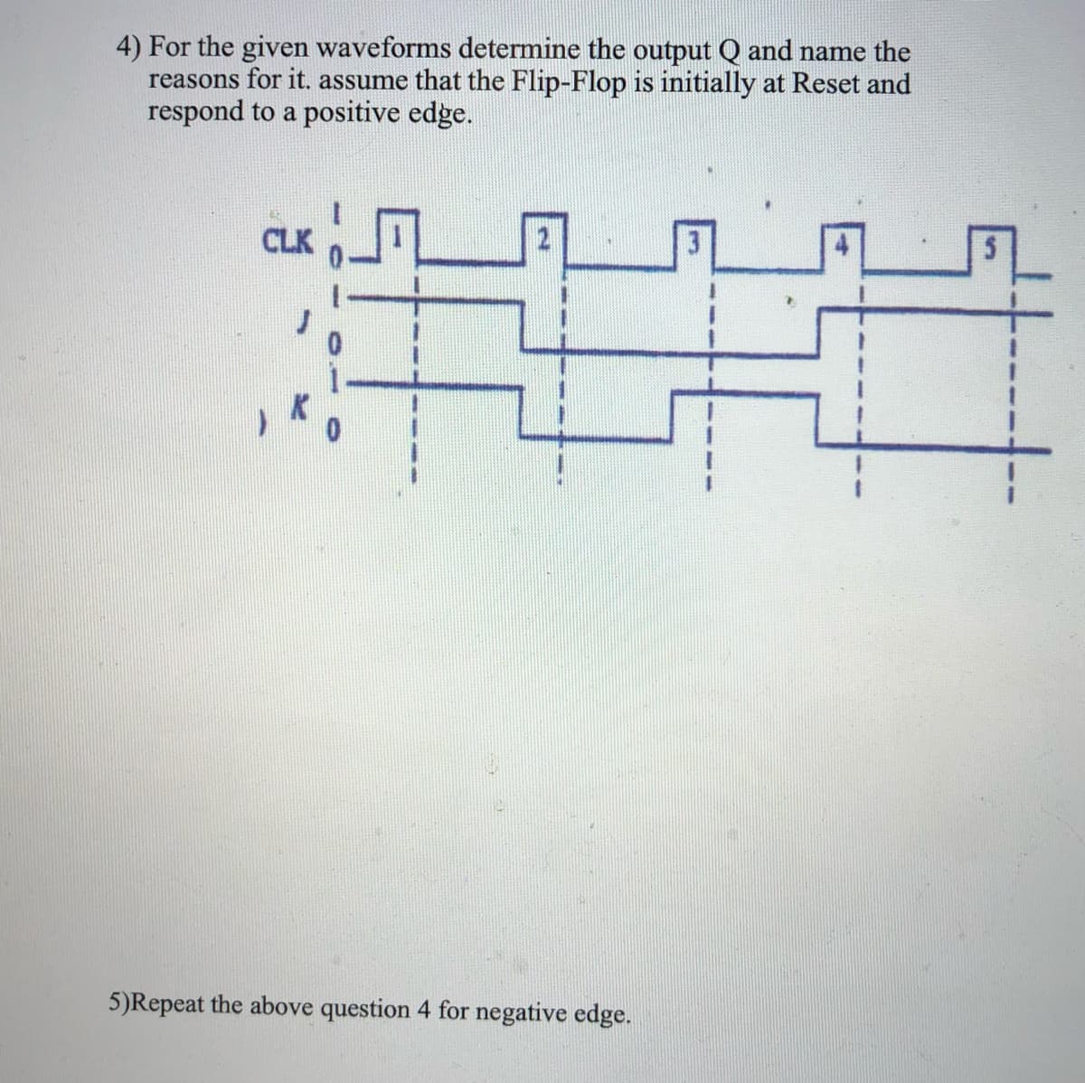
Transcribed Image Text:4) For the given waveforms determine the output Q and name the
reasons for it. assume that the Flip-Flop is initially at Reset and
respond to a positive edge.
CLK
5)Repeat the above question 4 for negative edge.
Expert Solution
This question has been solved!
Explore an expertly crafted, step-by-step solution for a thorough understanding of key concepts.

Step by step
Solved in 4 steps with 4 images

Knowledge Booster


Learn more about
Need a deep-dive on the concept behind this application? Look no further. Learn more about this topic, electrical-engineering and related others by exploring similar questions and additional content below.Recommended textbooks for you